
8-Inch vs 12-Inch Wafer Processing
Explore the key differences between 8-inch and 12-inch wafer processing, including manufacturing costs, yield considerations, equipment requirements, and backend implications for semiconductor production.
Kiran
1/5/20265 min read
The transition from 8-inch (200 mm) to 12-inch (300 mm) wafer processing represents one of the most consequential shifts in modern semiconductor manufacturing. While the industry narrative often frames this change as a simple scaling exercise driven by cost reduction, the practical reality is far more nuanced. Wafer diameter impacts equipment architecture, process windows, yield behavior, factory economics, and even long-term technology roadmaps.
Today, both 8-inch and 12-inch wafers coexist across logic, memory, power devices, MEMS, sensors, and specialty semiconductor markets. Understanding why—and knowing how to choose between them—requires a clear view of the technical and operational trade-offs involved.
Evolution of Wafer Sizes in Semiconductor Manufacturing
From 150 mm to 200 mm to 300 mm
Wafer size progression has historically followed a predictable cadence, driven by the need to increase die output per processing step while spreading fixed manufacturing costs over a larger area. The move from 150 mm to 200 mm wafers accelerated through the 1990s, enabling higher throughput and more efficient fab utilization.
The subsequent transition to 300 mm wafers in the early 2000s was more disruptive. Equipment had to be completely redesigned, automation became mandatory, and capital expenditure increased dramatically. However, the economic incentive—roughly 2.25× more surface area per wafer—ultimately justified the investment for high-volume manufacturing.
Why 8-Inch Still Matters
Despite the dominance of 12-inch fabs in advanced logic and memory, 8-inch wafer processing remains strategically important. Many analog, power, RF, MEMS, and specialty devices are optimized for mature nodes where process stability, equipment availability, and lower capital intensity outweigh raw scaling benefits.
In many cases, the device architecture or market demand simply does not justify a migration to 12-inch, particularly when volumes are moderate and margins depend on flexibility rather than scale.
Physical and Geometric Differences Between 8-Inch and 12-Inch Wafers
Surface Area and Die Economics
A 12-inch wafer provides approximately 70,685 mm² of usable surface area, compared to about 31,416 mm² for an 8-inch wafer. In theory, this allows more than twice the number of dies per wafer. In practice, edge exclusion, scribe lanes, and defect density distributions moderate the gain.
For large die designs, the benefit can be substantial. For small or irregular dies, the economic advantage may be less pronounced, particularly if yield variability increases.
Thickness, Flatness, and Mechanical Behavior
Larger wafers introduce stricter requirements for flatness, bow, and warp control. A 12-inch wafer experiences higher gravitational sag and greater sensitivity to thermal stress, making mechanical handling and thermal uniformity significantly more challenging.
These effects propagate downstream, influencing lithography overlay accuracy, film stress management, and backend handling during thinning, bonding, and dicing operations.
Equipment and Process Tooling Differences
Capital Equipment Architecture
12-inch tools are not scaled versions of 8-inch tools; they are fundamentally different systems. Robotics, vacuum chambers, heating elements, and gas flow designs must all accommodate the increased wafer mass and diameter.
As a result, 12-inch equipment carries substantially higher acquisition and maintenance costs. This makes economic sense for high-volume manufacturing but creates a barrier for smaller manufacturers or specialty device producers.
Automation and Material Handling
Manual or semi-automated handling is common in 8-inch fabs, particularly in R&D or low-volume environments. In contrast, 12-inch fabs are fully automated by necessity. Front-opening unified pods (FOUPs), overhead transport systems, and robotic wafer handling reduce contamination and improve repeatability but increase system complexity.
This automation improves consistency but reduces process flexibility and increases changeover time for non-standard flows.
Process Integration and Yield Considerations
Process Uniformity and Control
Achieving uniform deposition, etch, and thermal processing across a 300 mm wafer requires tighter control of process parameters and tool calibration. Minor non-uniformities that are negligible on 200 mm wafers can translate into significant yield loss on larger substrates.
Advanced process control (APC) and in-line metrology become mandatory at 12-inch scale, increasing both operational overhead and data complexity.
Defect Density Scaling
Defect density does not scale linearly with wafer area. Even with equivalent defect densities per unit area, the probability of a killer defect affecting at least one die increases with wafer size.
This places greater emphasis on contamination control, tool maintenance, and statistical process monitoring in 12-inch fabs, particularly for large-die applications.
Cost Structure and Manufacturing Economics
Cost Per Wafer vs Cost Per Die
While a 12-inch wafer costs significantly more to process than an 8-inch wafer, the cost per die is typically lower at sufficient volume. The break-even point depends on device size, yield, equipment depreciation, and utilization rates.
For high-volume products with stable designs, 12-inch processing delivers clear economic advantages. For lower-volume or highly customized devices, 8-inch processing often remains more cost-effective.
Fab Utilization and Legacy Infrastructure
Many 8-inch fabs are fully depreciated, allowing manufacturers to operate with lower overhead. Equipment availability on the secondary market further reduces capital barriers. In contrast, 12-inch fabs require sustained high utilization to justify their cost structure.
This dynamic explains why mature-node capacity constraints often emerge in 8-inch fabs, even as advanced 12-inch capacity expands.
Factory Operations and Supply Chain Considerations (NEW SECTION)
Beyond pure process economics, wafer size influences factory resilience and supply chain risk. The global semiconductor shortages of recent years exposed how heavily many industries depend on aging 8-inch capacity for power management ICs, automotive sensors, and industrial controllers.
Because 8-inch equipment is no longer manufactured at scale, tool availability, spare parts, and maintenance expertise have become strategic constraints. Conversely, 12-inch fabs rely on a narrower set of highly specialized suppliers, creating different—but equally critical—dependencies.
From an operational standpoint, 8-inch fabs often excel in mixed-product manufacturing, frequent changeovers, and rapid customer response. 12-inch fabs prioritize throughput stability, statistical control, and long production runs. These operational differences strongly influence how manufacturers structure their supply chains and customer commitments.
Backend Manufacturing and Advanced Packaging Implications
Wafer Thinning and Handling
12-inch wafers are typically thinned to comparable or even lower thicknesses than 8-inch wafers, increasing the risk of breakage, warpage, and handling-induced defects. Temporary bonding, carrier wafers, and advanced handling solutions are more frequently required.
These complexities extend into backend processes such as redistribution layer (RDL) formation, wafer-level packaging, and die singulation.
Packaging Ecosystem Compatibility
Not all backend tools and packaging flows are equally optimized for 12-inch wafers. Some advanced packaging techniques—particularly those developed initially for MEMS or power devices—remain more mature in 8-inch formats.
As heterogeneous integration and chiplet-based architectures expand, both wafer sizes continue to play complementary roles in the backend ecosystem.
Choosing Between 8-Inch and 12-Inch Wafer Processing
Application-Driven Decision Making
The choice between 8-inch and 12-inch processing is rarely binary. It depends on device type, production volume, lifecycle expectations, and supply chain considerations.
High-volume digital ICs naturally gravitate toward 12-inch fabs, while analog, power, and specialty devices often remain on 8-inch lines for decades.
Risk, Flexibility, and Time-to-Market
8-inch fabs offer faster process iteration, easier tool modification, and lower financial risk—advantages that matter during product development and early production phases. 12-inch fabs excel once designs are frozen and volume ramps justify the investment.
Successful manufacturers align wafer size strategy with both technical requirements and business realities.
Backend Manufacturing Support with Silicon Craft Technologies
As wafer sizes increase and backend processes become more complex, the distinction between front-end scaling and backend execution continues to blur. Silicon Craft Technologies brings an engineering-driven approach to backend semiconductor manufacturing that aligns with the practical challenges discussed throughout this article.
With experience supporting both 8-inch and 12-inch wafer flows, Silicon Craft Technologies works closely with customers on process development, advanced packaging support, and low-to-medium volume production. This includes wafer-level and package-level backend operations where mechanical handling, yield optimization, and process flexibility are critical.
By focusing on collaboration, process understanding, and manufacturability rather than rigid volume-driven models, Silicon Craft Technologies provides backend manufacturing support that complements a wide range of wafer size strategies—from mature 8-inch platforms to advanced 12-inch integrations.
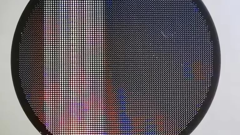
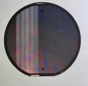
8-inch semiconductor wafer with patterned integrated circuits
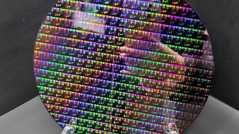
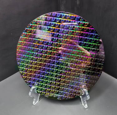
12-inch semiconductor wafer used in advanced chip manufacturing