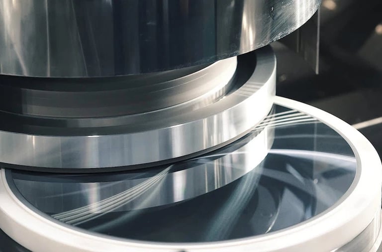
Wafer Backgrinding
Si-Craft Technologies provides precision backgrinding and lapping for wafers up to 12 inches, covering silicon, GaAs, GaN, InP, glass, and ceramic substrates. Our process achieves total thickness variation (TTV) below 5 µm with excellent planarity and controlled surface roughness (Ra < 10 nm, depending on material and process flow). Capabilities include ultra-thin grinding to below 100 µm, partial thinning, and multi-step grind/lap sequences to ensure high wafer integrity, minimal subsurface damage, and optimal conditions for dicing.