
Best Practices for Handling Ultra-Thin Wafers in Back-End Manufacturing
Learn essential best practices for handling ultra-thin wafers in back-end manufacturing to reduce breakage, improve yield, and ensure reliable semiconductor assembly.
Kiran
1/5/20265 min read
As semiconductor devices continue to evolve toward higher performance, lower power consumption, and advanced packaging architectures, wafer thinning has become a critical enabler. Ultra-thin wafers—often below 100 µm and, in some applications, below 50 µm—are now common in fan-out packaging, 3D integration, power devices, and heterogeneous systems. While thinning enables electrical and thermal advantages, it also introduces significant mechanical risk during back-end manufacturing.
Handling ultra-thin wafers requires a fundamentally different approach compared to conventional backend processing. Mechanical fragility, warpage sensitivity, and process-induced stress all increase dramatically as wafer thickness is reduced. Without well-defined handling strategies, yield loss can occur through cracking, chipping, excessive warpage, or latent reliability failures.
This article outlines best practices for handling ultra-thin wafers in back-end manufacturing, focusing on practical measures that improve yield, stability, and manufacturability across real production environments.
Why Ultra-Thin Wafers Are Challenging in Back-End Processing
The primary challenge with ultra-thin wafers is the loss of mechanical stiffness. As thickness decreases, the wafer’s ability to resist bending and localized stress diminishes rapidly. Forces that are negligible for standard-thickness wafers—such as vacuum chucking, thermal gradients, or minor handling misalignment—can become destructive.
In backend manufacturing, wafers are exposed to multiple risk factors simultaneously: grinding and polishing, temporary bonding and debonding, cleaning, inspection, dicing, and assembly. Each step introduces mechanical or thermal stress that accumulates across the process flow. Managing these stresses holistically is essential to prevent catastrophic and latent failures.
Wafer Thinning Strategy and Stress Management
Controlled Thinning Processes
Backgrinding is the most common thinning method, but it is also a major source of stress. Best practice involves using a multi-step grinding approach, starting with coarse removal followed by progressively finer grinding and polishing steps. This reduces subsurface damage and minimizes stress concentration.
Uniform material removal is critical. Non-uniform grinding thickness translates directly into curvature and warpage, increasing handling risk downstream. Equipment calibration, wheel condition, and process repeatability must be tightly controlled.
Stress Relief Considerations
Ultra-thin wafers often retain residual stress after thinning. Where possible, low-temperature stress relief steps or controlled dwell times should be incorporated before proceeding to subsequent backend operations. Abrupt transitions between thinning and high-stress steps increase the likelihood of wafer deformation or fracture.
Temporary Wafer Support and Carrier Strategies
Importance of Temporary Support
For wafers below a critical thickness, free-standing handling is impractical. Temporary wafer bonding to a rigid carrier provides the mechanical stability required for safe backend processing. This approach distributes stress more evenly and enables compatibility with standard handling equipment.
Carrier selection should account for thermal expansion compatibility, stiffness, and surface flatness. Mismatches between the wafer and carrier can introduce new stress during thermal cycling.
Bonding and Debonding Best Practices
Bonding materials and processes must be selected based on the full backend thermal and chemical exposure profile. Inadequate bonding can lead to local delamination, while overly aggressive bonding can complicate clean debonding and introduce residual warpage.
Debonding is a particularly sensitive step. Mechanical forces, thermal gradients, or laser-based release methods must be carefully tuned to avoid inducing cracks or sudden stress release. Post-debond inspection and flatness verification are essential before assembly.
Handling Equipment and Automation Adaptation
Vacuum Chucking and Contact Forces
Standard vacuum chuck designs may not be suitable for ultra-thin wafers. Excessive vacuum pressure can locally deform or fracture the wafer, while uneven vacuum distribution exacerbates warpage.
Best practice includes using low-pressure, zoned, or compliant vacuum chucks that distribute force uniformly. Where possible, mechanical contact should be minimized, and handling speeds should be reduced to lower dynamic stress.
Automation Speed and Acceleration Control
High-speed automation optimized for thicker wafers can introduce inertial forces that exceed the mechanical limits of ultra-thin substrates. Slower acceleration profiles, gentler pick-and-place motions, and tighter positional control reduce the risk of micro-cracks and edge damage.
Although these adjustments may reduce throughput, they often result in net productivity gains by reducing breakage and rework.
Warpage Control During Backend Operations
Warpage Monitoring
Ultra-thin wafers are inherently more sensitive to warpage caused by residual stress, film deposition, and thermal cycling. Continuous monitoring of wafer flatness at key backend stages—after thinning, after debonding, and before assembly—provides early warning of process excursions.
Relying solely on end-of-line measurements limits corrective options. In-process monitoring enables proactive adjustments.
Thermal Budget Management
Even moderate temperature excursions can significantly alter wafer curvature at reduced thickness. Backend processes should minimize thermal gradients and avoid unnecessary high-temperature exposure. Controlled ramp rates and uniform heating are critical to maintaining flatness.
Cleaning, Inspection, and Metrology Considerations
Ultra-thin wafers require modified cleaning and inspection protocols. High-pressure fluid jets, aggressive brush cleaning, or excessive mechanical contact can damage thin substrates.
Non-contact or low-force cleaning methods are preferred, and inspection systems must accommodate increased wafer bow without introducing handling stress. Optical focus and alignment systems should be configured to account for curvature variation across the wafer surface.
Dicing and Singulation Best Practices
Singulation is one of the highest-risk steps for ultra-thin wafers. Traditional sawing methods can introduce edge chipping and crack propagation if not optimized.
Best practices include:
Optimized blade selection and feed rates
Enhanced wafer support during cutting
Alternative singulation techniques where applicable, such as laser dicing
Post-dicing inspection is critical, as micro-cracks introduced at this stage may not be immediately visible but can cause downstream assembly or reliability failures.
Assembly and Packaging Integration
Ultra-thin wafers impose tighter tolerances during die attach and interconnect formation. Planarity variations affect placement accuracy, solder joint formation, and bond integrity.
Assembly tools should be configured to accommodate residual curvature, using compliant interfaces or adaptive force control where possible. Process windows must be validated using wafers that reflect real warpage distributions rather than idealized flat samples.
Yield, Reliability, and Economic Considerations
Yield loss associated with ultra-thin wafer handling often appears indirectly. Breakage, rework, increased cycle time, and reduced equipment utilization all contribute to higher cost of ownership.
From an economic standpoint, investments in proper handling infrastructure—temporary bonding systems, compliant tooling, enhanced metrology—are often justified by improved yield stability and reduced latent reliability risk.
Ultra-thin wafer handling should be treated as a yield-critical discipline, not an afterthought.
Building a Robust Ultra-Thin Wafer Handling Strategy
Successfully handling ultra-thin wafers in back-end manufacturing requires an integrated strategy that spans equipment, materials, process sequencing, and organizational alignment. Isolated optimizations are rarely sufficient; stress introduced in one step often manifests as failure in another.
Cross-functional collaboration between process engineering, equipment engineering, and assembly teams is essential. Clear ownership of mechanical integrity and consistent feedback loops enable continuous improvement as wafer thickness targets continue to shrink.
Backend Manufacturing Support with Silicon Craft Technologies
Ultra-thin wafer handling presents complex challenges that span thinning, temporary support, backend processing, and assembly integration. Addressing these challenges requires not only appropriate tools, but also a deep understanding of how mechanical behavior evolves across the manufacturing flow.
Silicon Craft Technologies supports backend manufacturing by working closely with customers to develop handling strategies tailored to ultra-thin wafers and advanced packaging requirements. Through process development, prototyping, and low-to-medium volume manufacturing support, Si-Craft helps identify stress drivers early and implement practical mitigation measures aligned with real production constraints.
By integrating mechanical considerations into backend process development, Silicon Craft Technologies enables more predictable yield, improved reliability, and scalable handling solutions as device architectures continue to advance.
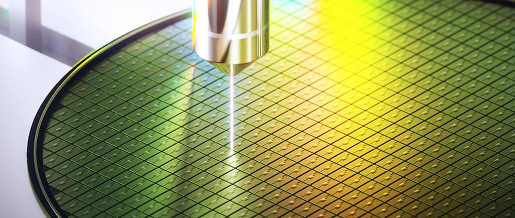
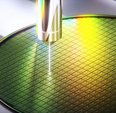
“Laser processing step on a silicon wafer during advanced semiconductor wafer manufacturing”