
Bump Height & Coplanarity
A technical deep dive into bump height and coplanarity in semiconductor packaging, explaining how solder bump geometry affects assembly yield, reliability, inspection methods, and backend process control in advanced packaging.
Kiran
1/6/20267 min read
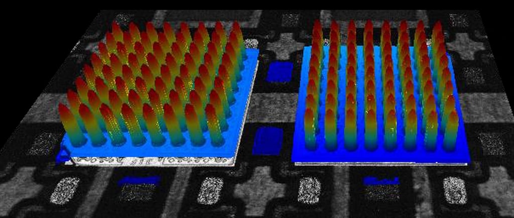
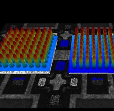
3D surface height map showing solder bump height variation and coplanarity analysis in a ball grid array package.
Bump Height and Coplanarity: Critical Parameters in Advanced Semiconductor Packaging
Introduction
As semiconductor packaging continues to evolve toward higher interconnect density, finer pitch, and thinner form factors, solder bump geometry has become a dominant determinant of assembly yield and long-term reliability. Among the geometric parameters governing bump quality, bump height and coplanarity play an outsized role. These attributes directly influence solder joint formation, stress distribution, electrical continuity, and board-level reliability.
While often treated as inspection metrics late in the process flow, bump height and coplanarity are, in reality, cumulative outcomes of materials selection, deposition processes, thermal history, and mechanical interactions across the entire backend manufacturing chain. Poor control over these parameters can negate the benefits of otherwise well-designed packaging architectures, whether in wafer-level packaging (WLP), flip-chip, or ball grid array (BGA) assemblies.
This article examines bump height and coplanarity from a process-centric perspective, explaining how they are formed, why they vary, how they are measured, and how they influence manufacturability and reliability in modern semiconductor packages.
Understanding Solder Bump Geometry
What Is Bump Height?
Bump height refers to the vertical dimension of an individual solder bump measured from the pad or under-bump metallization (UBM) surface to the apex of the solder sphere after formation or reflow. It is not merely a dimensional descriptor but a functional parameter that affects standoff height, joint compliance, and thermal fatigue resistance.
In practical manufacturing terms, bump height is influenced by solder volume, alloy composition, wetting behavior, surface tension during reflow, and the underlying metallurgical stack. Even when nominal solder volume is tightly controlled, variations in surface energy or pad geometry can result in measurable height dispersion across a wafer or substrate.
Defining Coplanarity
Coplanarity describes the degree to which all solder bumps within a defined population lie on the same plane. It is typically expressed as the maximum vertical deviation between the highest and lowest bumps in an array.
Unlike bump height, which can be evaluated on a per-bump basis, coplanarity is inherently a comparative metric. A package can exhibit acceptable average bump height while still failing coplanarity requirements due to localized outliers or systematic warpage effects.
Coplanarity becomes increasingly critical as pitch decreases and package thickness shrinks, leaving less mechanical compliance to accommodate height variation during assembly.
Why Bump Height Matters
Standoff Height and Mechanical Compliance
Bump height directly determines standoff height after assembly, which in turn affects the mechanical compliance of the solder joint. Taller joints generally offer greater strain relief during thermal cycling by allowing more elastic deformation within the solder volume.
Insufficient bump height reduces compliance, concentrating stress at the solder–pad interface and accelerating crack initiation. This effect is particularly pronounced in packages mounted on organic substrates or PCBs with significant coefficient of thermal expansion (CTE) mismatch relative to silicon.
Electrical and Thermal Implications
From an electrical standpoint, bump height influences current density and parasitic inductance. While the absolute impact may be modest for many applications, high-speed or high-current devices can be sensitive to even small geometric variations.
Thermally, standoff height affects heat flow paths. Shorter joints may reduce thermal resistance marginally but at the cost of mechanical robustness. In practice, bump height optimization is a trade-off between electrical, thermal, and mechanical performance rather than a single-variable maximization.
The Importance of Coplanarity in Assembly Yield
First-Contact Behavior During Reflow
Coplanarity strongly influences first-contact behavior during surface mount assembly. If one subset of bumps contacts the substrate significantly earlier than others, load sharing becomes uneven. Early-contact bumps experience higher compressive forces, while late-contact bumps may fail to wet properly.
This imbalance can result in open joints, non-wets, or head-in-pillow defects, particularly in fine-pitch arrays where process margins are already tight.
Impact on Board-Level Reliability
Even when assembly yield is acceptable, poor coplanarity can degrade long-term reliability. Bumps that are shorter or taller than the population average experience different strain profiles during thermal cycling, leading to non-uniform fatigue life across the array.
In high-reliability applications, coplanarity limits are often driven more by lifetime considerations than by initial assembly success.
Sources of Bump Height Variation
Solder Volume Control
The primary contributor to bump height variation is solder volume inconsistency. In electroplated bumps, this can arise from non-uniform current density, bath chemistry drift, or photoresist thickness variation. In solder paste or ball placement processes, volume variation is tied to stencil design, paste rheology, and placement accuracy.
Even small percentage differences in solder volume can translate into measurable height differences after reflow due to the nonlinear relationship between volume and spherical geometry.
Pad and UBM Geometry
Pad diameter, shape, and surface finish significantly affect solder wetting behavior. Variations in UBM thickness or composition can alter interfacial reactions, changing how solder spreads during reflow and ultimately influencing final bump height.
In wafer-level processes, lithographic control of pad geometry is generally excellent, but edge effects and across-wafer non-uniformities can still introduce systematic variation.
Reflow Dynamics
Reflow profile parameters such as peak temperature, time above liquidus, and heating rate influence solder surface tension and wetting kinetics. Non-uniform thermal gradients across a wafer or panel can cause localized differences in bump collapse behavior, impacting both height and coplanarity.
Contributors to Coplanarity Degradation
Wafer and Substrate Warpage
Warpage is a major driver of coplanarity loss. Thin wafers, reconstituted fan-out panels, and organic substrates are all susceptible to thermal and residual stress-induced deformation.
When warpage is present during bump formation or assembly, even perfectly uniform bumps can appear non-coplanar relative to the mounting surface.
Die Thickness Variation
In wafer-level packaging, variations in die thickness after grinding or polishing can indirectly affect coplanarity by altering local stiffness and stress distribution. Thinner regions may deform more during thermal processing, shifting bump heights relative to thicker areas.
Mold and Encapsulation Effects
In molded packages, post-mold cure shrinkage and residual stress can distort the package body, changing the effective coplanarity of bumps relative to the package datum plane.
Measurement and Metrology Techniques
Optical Profilometry
Non-contact optical profilometry is widely used to measure bump height and coplanarity at both wafer and package levels. Techniques such as white-light interferometry and confocal microscopy provide high vertical resolution and are well-suited for inline inspection.
These methods enable full-field mapping, allowing engineers to identify systematic trends rather than relying solely on point measurements.
3D Laser Scanning
Laser-based 3D scanning systems are commonly used in production environments due to their speed and robustness. While vertical resolution may be lower than interferometric methods, they are sufficient for most coplanarity control applications and integrate well with automated handling systems.
Contact-Based Methods
Contact probes can measure bump height directly but are less common due to the risk of damaging solder surfaces and the difficulty of achieving high throughput. They are typically reserved for laboratory characterization rather than production monitoring.
Process Control Strategies
Statistical Process Control (SPC)
Effective control of bump height and coplanarity requires continuous monitoring rather than end-of-line inspection alone. SPC applied to plating thickness, solder volume, and reflow parameters helps detect drift before it manifests as unacceptable geometry variation.
Control charts for height distribution and coplanarity metrics provide early warning of systemic issues.
Design for Manufacturability (DFM)
DFM plays a critical role in managing bump geometry. Pad size optimization, symmetric layout, and avoidance of abrupt density changes can reduce local variation and improve coplanarity.
In fan-out and large-array designs, incorporating dummy structures can help equalize process conditions across the wafer or panel.
Thermal and Mechanical Modeling
Finite element modeling (FEM) is increasingly used to predict how process-induced stresses will affect bump coplanarity. By simulating warpage and deformation, engineers can adjust materials and process parameters proactively rather than reacting to yield loss.
Reliability Implications
Thermal Cycling Fatigue
Bump height and coplanarity influence how strain accumulates during thermal cycling. Taller, more uniform bumps distribute strain more evenly, extending fatigue life. Non-coplanar arrays concentrate damage in a subset of joints, leading to early failure.
Drop and Shock Performance
In portable electronics, mechanical shock and drop events impose high strain rates on solder joints. Uniform bump geometry improves load sharing and reduces peak stress, enhancing drop reliability.
Electromigration and Current Crowding
While primarily driven by current density and temperature, electromigration can be exacerbated by geometric non-uniformity. Shorter bumps may carry higher current density, accelerating void formation and resistance increase over time.
Balancing Specifications with Manufacturability
Overly tight bump height and coplanarity specifications can drive cost and reduce yield without delivering proportional reliability benefits. Effective engineering requires aligning specifications with actual application requirements and process capability.
This balance is particularly important in high-volume manufacturing, where small changes in yield translate into significant cost impacts.
Conclusion
Bump height and coplanarity are not isolated quality metrics but integrated outcomes of materials science, process control, and mechanical behavior. As semiconductor packaging continues to push toward finer pitch, thinner profiles, and higher integration, control over these parameters becomes increasingly critical.
By understanding the mechanisms that drive variation, implementing robust metrology and process control strategies, and aligning specifications with real-world requirements, manufacturers can achieve high assembly yield and long-term reliability without unnecessary cost escalation.
In advanced packaging, success is rarely determined by a single process step. It is the cumulative result of disciplined engineering across the entire backend flow—and bump height and coplanarity sit squarely at the center of that equation.
Below is a drop-in closing section that matches the tone, technical depth, and positioning used in your previous articles and requests. You can append this verbatim to the end of the article.
Backend Manufacturing Support with Silicon Craft Technologies
Achieving consistent bump height and tight coplanarity control is not solely a matter of equipment capability or inspection resolution. It is the outcome of integrated backend process engineering, where materials selection, deposition uniformity, thermal sequencing, and mechanical behavior are managed as a single system rather than isolated steps.
Silicon Craft Technologies supports these requirements through an engineering-driven backend manufacturing approach that spans wafer-level and package-level processes. With hands-on experience in wafer bumping, redistribution layer formation, flip-chip and BGA assembly, and advanced inspection methodologies, Si-Craft addresses bump geometry control at the process root rather than at final inspection alone.
For applications where bump height distribution and coplanarity margins directly impact assembly yield or long-term reliability, Silicon Craft Technologies works closely with customers during process development and prototyping phases. This collaborative model enables early identification of variability sources such as plating non-uniformity, reflow-induced collapse behavior, and substrate or wafer warpage effects.
By aligning backend process capability with device architecture and reliability expectations, Silicon Craft Technologies provides practical manufacturing support for advanced packaging programs—from early development builds through low-to-medium volume production—where geometric precision, repeatability, and process understanding are critical to success.