
Common Wafer Defects in Back-End Processing
Explore the most common wafer defects in back-end semiconductor processing, their root causes, and practical strategies to detect, prevent, and improve manufacturing yield.
Kiran
1/5/202611 min read
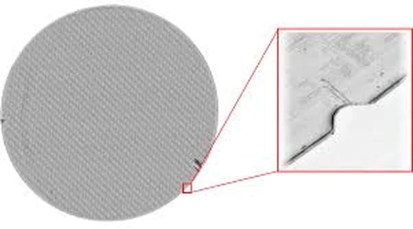
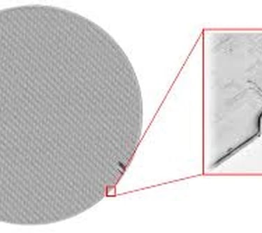
This image shows a crystalline defect identified during wafer inspection, highlighting common material and stress-related issues that can impact yield and reliability in back-end semiconductor processing.
Back-end semiconductor processing is often perceived as mechanically simpler than front-end wafer fabrication, yet it introduces a distinct and highly consequential class of wafer defects. As wafers move from fully processed substrates into thinning, bonding, dicing, and packaging workflows, mechanical stress, material interactions, and handling variability become dominant yield drivers. Unlike front-end defects, which are frequently rooted in lithography or process chemistry, back-end defects are strongly influenced by physical forces, tool interfaces, and cumulative process history.
This article provides a comprehensive technical examination of common wafer defects in back-end processing, focusing on their root causes, failure mechanisms, detection methods, and practical mitigation strategies. The discussion is framed for process engineers, manufacturing leaders, and advanced packaging specialists working across wafer-level and package-level backend operations.
Understanding Back-End Processing and Defect Sensitivity
Back-end processing encompasses all manufacturing steps following front-end device fabrication, including wafer thinning, cleaning, temporary and permanent bonding, redistribution layer (RDL) formation, singulation, die attach, and final packaging. At this stage, wafers are structurally weaker, thinner, and more vulnerable to damage than at any earlier point in the manufacturing flow.
Several factors make back-end processes uniquely defect-sensitive:
Reduced wafer thickness, often below 100 µm
Cumulative residual stress from front-end films and thermal cycles
Increased mechanical handling, including contact-based tooling
Heterogeneous material interfaces, such as adhesives, carriers, and metals
Tighter tolerance for cosmetic and mechanical defects, particularly for advanced packaging
Defects introduced during back-end processing are especially problematic because they frequently appear late in the manufacturing cycle, after significant value has already been added to the wafer.
Classification of Common Back-End Wafer Defects
Back-end wafer defects can be broadly classified into several categories based on their physical nature and origin:
Mechanical defects
Surface defects
Structural and crystalline defects
Contamination-related defects
Process-induced warpage and deformation
Singulation and edge-related defects
Each category has distinct root causes, inspection challenges, and yield implications. Importantly, many back-end defects are not isolated events but are the cumulative result of earlier process interactions.
Mechanical Defects: Cracks, Chips, and Fractures
Wafer Cracking
Cracking is among the most severe and yield-limiting defects encountered during back-end processing. Cracks may initiate at the wafer edge, propagate radially, or develop internally due to stress concentration.
Common causes include:
Excessive wafer thinning without adequate support
Improper chuck vacuum distribution
Thermal mismatch between wafer and carrier materials
High localized stress during debonding or dicing
Cracks are particularly dangerous because they may remain undetected until late-stage inspection or even post-assembly reliability testing. In extreme cases, cracks can propagate during normal package use, leading to field failures.
Edge Chipping
Edge chipping occurs when small fragments break away from the wafer perimeter. While often considered cosmetic, edge chips can act as stress concentrators and crack initiation sites.
Edge chipping is commonly associated with:
Inadequate edge protection during thinning
Poor blade alignment during dicing
Mechanical shock during handling or transport
As wafer thickness decreases, susceptibility to edge chipping increases significantly, especially for large-diameter wafers.
Surface Defects Introduced During Back-End Processing
Scratches and Abrasion Marks
Surface scratches are frequently introduced during wafer handling, cleaning, or contact with tooling surfaces. While some scratches are superficial, deeper abrasions can penetrate active layers or redistribution structures.
Typical contributors include:
Contaminated handling tools or carriers
Improper cleaning brush pressure
Misaligned robotic end-effectors
Residual particles between wafer and chuck surfaces
Scratches are particularly critical for wafers undergoing wafer-level packaging or RDL processes, where surface integrity is essential for adhesion and electrical performance.
Residue and Staining
Back-end cleaning processes are designed to remove particulates, adhesives, and process residues, but incomplete or poorly controlled cleaning can introduce new defects. Residue stains may originate from:
Inadequate rinse steps
Chemical incompatibility with exposed materials
Drying non-uniformities
Degraded cleaning chemistries
While some residues are benign, others can interfere with bonding, metallization, or inspection accuracy.
Structural and Crystalline Defects in Back-End Contexts
Although crystalline defects are often associated with front-end processing, back-end steps can exacerbate or reveal pre-existing structural weaknesses. Mechanical stress during thinning or bonding can activate latent defects such as dislocations or slip lines.
Crystalline-related defects may appear as:
Slip bands induced by thermal stress
Microcracks along crystallographic planes
Stress-enhanced dislocation movement
These defects are especially relevant for power devices and compound semiconductor wafers, where crystal integrity is closely tied to electrical performance and long-term reliability.
Warpage and Bow: Deformation-Induced Defects
Wafer warpage and bow are increasingly critical concerns in back-end processing, particularly for advanced packaging applications. Warpage arises from stress imbalance across the wafer thickness, often caused by:
Asymmetric film stacks
Temporary bonding adhesives
Thermal excursions during curing or annealing
Carrier mismatch in temporary bonding schemes
Excessive warpage can lead to:
Poor tool contact and vacuum sealing
Non-uniform thinning
Misalignment during lithography-based backend steps
Increased risk of cracking during debonding
Controlling warpage requires a holistic understanding of material properties, thermal budgets, and process sequencing.
Inspection Challenges in Back-End Defect Detection
Detecting back-end wafer defects presents unique challenges. As wafers become thinner and more fragile, traditional inspection techniques may introduce additional risk.
Common inspection methods include:
Optical inspection for surface and edge defects
Infrared imaging for subsurface cracks
Acoustic microscopy for delamination and voids
Stress and warpage measurement tools
Each technique has limitations, and effective defect detection often requires a combination of methods tailored to the specific process flow.
Contamination-Related Defects in Back-End Processing
Contamination in back-end processing differs fundamentally from front-end contamination. While front-end contamination is often sub-micron and electrically driven, backend contamination is frequently mechanical, chemical, or organic in nature, and directly affects bonding integrity, surface quality, and reliability.
Particle Contamination
Particles introduced during backend processing can originate from multiple sources:
Grinding wheels and polishing pads
Degraded temporary bonding adhesives
Carrier wafer surfaces
Tool wear debris
Inadequate post-process cleaning
Particles trapped between the wafer and carrier during temporary bonding can create localized stress points, leading to thickness non-uniformity, microcracking, or imprint defects that replicate through subsequent layers.
Even relatively large particles—tens of microns in size—can be catastrophic when wafers are thinned below 100 µm, as the wafer loses the ability to elastically accommodate surface asperities.
Organic Contamination and Residues
Organic contamination is particularly problematic in back-end flows that involve adhesives, tapes, and polymers. Common sources include:
Temporary bonding adhesives
Dicing tapes
Photoresist residues from RDL processes
Outgassing from carriers or fixtures
Residual organic films can interfere with:
Permanent bonding strength
Metal adhesion in RDL layers
Die attach quality
Long-term package reliability
Unlike particulate contamination, organic residues are often difficult to detect optically and may only be revealed through poor process performance or reliability failures.
Temporary Bonding and Debonding Defects
Temporary bonding has become a cornerstone of advanced backend processing, enabling ultra-thin wafer handling and complex wafer-level packaging. However, it also introduces a distinct set of defect risks.
Bond Voids and Non-Uniform Adhesion
Non-uniform adhesive coverage during temporary bonding can result in voids or weakly bonded regions. These areas are highly susceptible to:
Localized wafer bending during thinning
Differential stress during thermal cycling
Delamination during debonding
Bond voids often manifest later as cracks, surface imprints, or thickness variations, making root-cause analysis challenging.
Adhesive Flow and Edge Bead Effects
Excessive adhesive flow during bonding or curing can create edge bead build-up, leading to:
Wafer edge distortion
Poor chuck sealing
Non-uniform thinning profiles
If not properly controlled, edge bead effects can propagate into downstream dicing and singulation defects.
Debonding-Induced Damage
Debonding is one of the highest-risk steps in backend processing. Depending on the debonding method—thermal, mechanical, or laser-assisted—wafer damage may include:
Sudden crack propagation
Surface tearing or adhesive residue
Localized thermal shock
Carrier-induced stress release
Debonding defects are often catastrophic and can result in total wafer loss if not carefully managed.
Wafer Thinning and Grinding Defects
Wafer thinning is central to modern packaging but is also one of the most defect-prone backend processes.
Grinding-Induced Subsurface Damage
Mechanical grinding introduces subsurface microcracks and lattice damage beneath the wafer surface. While polishing and stress relief steps aim to remove this damage, incomplete removal can leave residual flaws that later propagate.
Key contributors include:
Aggressive grind parameters
Worn grinding wheels
Insufficient intermediate polish steps
Subsurface damage is particularly dangerous because it may not be visible during standard inspection yet significantly reduces wafer strength.
Thickness Non-Uniformity (TTV)
Total thickness variation (TTV) is a critical metric in backend processing. Excessive TTV can lead to:
Warpage and bow
Poor bonding uniformity
Dicing depth errors
Die-to-die mechanical variability
TTV issues often arise from:
Chuck vacuum non-uniformity
Carrier flatness issues
Tool calibration drift
As wafer thickness decreases, tolerance to TTV tightens dramatically.
Stress Accumulation and Latent Defect Activation
A defining characteristic of back-end defects is their cumulative nature. Many defects introduced during backend processing are not entirely new, but rather the activation of latent weaknesses created earlier in the manufacturing flow.
Interaction with Front-End Film Stress
Front-end film stacks may contain residual tensile or compressive stress. When the wafer is thinned, these stresses are no longer mechanically balanced, increasing the likelihood of:
Wafer bow
Slip generation
Crack initiation
This interaction explains why wafers that appear stable during front-end processing may fail during backend steps.
Thermal Cycling Effects
Backend processes often involve repeated thermal excursions for curing, annealing, or bonding. These cycles can:
Accelerate crack growth
Worsen delamination
Increase warpage through CTE mismatch
Thermal history must therefore be considered holistically across both front-end and back-end flows.
Detection and Monitoring of Backend-Specific Defects
Effective control of backend defects relies on early detection and process monitoring.
Common monitoring techniques include:
In-line optical inspection for scratches, particles, and edge defects
Infrared inspection for subsurface cracks
Acoustic microscopy for delamination and voids
Warpage measurement after key process steps
Backend inspection strategies must balance detection sensitivity against the risk of introducing additional handling damage.
Dicing and Singulation-Induced Wafer Defects
Wafer dicing is one of the most mechanically aggressive steps in backend processing. Whether using blade dicing, laser dicing, or hybrid approaches, singulation introduces stress concentrations that can easily propagate pre-existing damage.
Chipping and Microcracking Along Dicing Streets
Chipping along the dicing streets is a common defect, particularly for ultra-thin wafers. Chipping may be visible immediately after dicing or may only become apparent after die handling.
Primary contributors include:
Blade wear or improper blade selection
Excessive feed rates
Insufficient cooling or debris removal
Poor alignment between dicing streets and device layout
Microcracks extending from dicing streets are especially dangerous because they can propagate during die attach or thermal cycling in the final package.
Delamination During Singulation
In wafer-level packaging flows, singulation may occur after multiple RDL or passivation layers have been deposited. Poor adhesion between these layers can lead to delamination at the die edges during dicing.
Delamination is often linked to:
Inadequate surface preparation prior to deposition
Contamination trapped between layers
Thermal mismatch between polymer and metal layers
Edge delamination can compromise moisture resistance and long-term package reliability.
Edge Defects and Edge Exclusion Challenges
Wafer edges are inherently more vulnerable than central regions due to geometry, handling exposure, and process non-uniformity.
Edge Cracks and Fracture Initiation
Edge cracks often originate from:
Wafer handling tools
Temporary bonding edge bead buildup
Grinding or polishing non-uniformity
Once initiated, edge cracks can propagate rapidly across the wafer, particularly during debonding or dicing.
Edge Exclusion and Yield Loss
Many backend processes exclude a certain edge region to avoid defects, but aggressive edge exclusion reduces usable die count. Balancing edge quality with die yield is an ongoing optimization challenge, especially for large-diameter wafers.
Wafer-Level Packaging–Specific Defects
Wafer-level packaging (WLP) introduces additional complexity and new defect modes that are not present in traditional backend flows.
Redistribution Layer (RDL) Defects
RDL processes involve multiple lithography, plating, and dielectric deposition steps on thinned wafers. Common RDL-related defects include:
Metal voids and opens
Dielectric cracking
Poor metal adhesion
Misalignment due to wafer warpage
These defects can lead to electrical failures that are difficult to repair or rework.
Under-Bump Metallization (UBM) Failures
UBM layers provide the mechanical and electrical interface between the wafer and solder bumps. Defects in UBM layers may result from:
Surface contamination
Improper deposition conditions
Thermal stress during reflow
UBM-related defects often manifest later as solder joint failures or intermittent electrical connections.
Reliability Implications of Back-End Wafer Defects
One of the most critical aspects of backend wafer defects is their impact on long-term device reliability.
Crack Propagation Over Time
Microcracks introduced during backend processing may not cause immediate yield loss but can propagate during:
Thermal cycling
Mechanical shock
Vibration during use
This delayed failure mechanism is particularly concerning for automotive, aerospace, and industrial applications.
Moisture Ingress and Corrosion
Surface and edge defects create pathways for moisture ingress, increasing the risk of corrosion, leakage currents, and electrical degradation.
Packages that pass initial electrical testing may still fail reliability qualification due to backend-induced defects.
Process Control Strategies for Defect Prevention
Preventing backend wafer defects requires a combination of robust process design, real-time monitoring, and disciplined handling practices.
Key strategies include:
Optimizing wafer thinning sequences to minimize subsurface damage
Carefully selecting temporary bonding materials and carriers
Implementing strict contamination control protocols
Monitoring warpage and stress after each critical step
Using inspection data to drive continuous process improvement
Importantly, backend defect control must be integrated with front-end process knowledge rather than treated as an isolated manufacturing stage.
Data-Driven Yield Improvement in Backend Processing
Advanced backend manufacturing increasingly relies on data analytics to identify defect trends and correlations.
By correlating:
Inspection data
Tool parameters
Wafer history
manufacturers can identify subtle interactions that lead to defect formation and proactively adjust process conditions.
As semiconductor manufacturing continues to evolve toward thinner wafers, advanced packaging, and heterogeneous integration, back-end defect control has become a primary determinant of yield and reliability. In this final section, we examine advanced mitigation techniques, future backend defect challenges, and conclude with a technically grounded perspective on backend manufacturing support.
Advanced Mitigation Techniques for Back-End Wafer Defects
Reducing back-end wafer defects requires more than isolated tool optimization. It demands a systems-level approach that considers materials, equipment, process sequencing, and cumulative stress effects.
Stress Engineering and Process Sequencing
One of the most effective ways to mitigate backend defects is through deliberate stress management. This includes:
Balancing front-end film stress prior to thinning
Sequencing thermal steps to minimize abrupt stress changes
Introducing stress-relief polishing or annealing steps
Process sequencing can significantly influence defect formation. For example, performing high-temperature curing before final thinning can reduce crack propagation risk by allowing stress relaxation while the wafer is still mechanically robust.
Material Selection and Compatibility
Material compatibility is a recurring theme in backend defect control. Temporary bonding adhesives, carrier wafers, dielectrics, and metals must be selected with consideration for:
Coefficient of thermal expansion (CTE) matching
Chemical compatibility during cleaning and etching
Mechanical stiffness and debonding behavior
Inadequate material matching often leads to warpage, delamination, and residual stress accumulation.
Tool Interface and Handling Optimization
Many backend defects originate not from the process chemistry or physics, but from how wafers interact with tools. Improvements in:
Chuck design
Vacuum distribution
End-effector materials
Contact pressure control
can dramatically reduce scratches, cracks, and handling-induced damage.
Backend Defect Challenges in Advanced Packaging and Heterogeneous Integration
Advanced packaging technologies introduce new backend defect risks that extend beyond traditional wafer processing.
Chiplets and Multi-Die Integration
Heterogeneous integration relies on the precise alignment and bonding of multiple dies, often fabricated on different wafers or technologies. Backend defects that might be tolerable in single-die packages can become catastrophic in chiplet architectures.
Key challenges include:
Cumulative warpage across multiple layers
Increased sensitivity to die edge defects
Higher mechanical stress at interconnect interfaces
Backend defect control must therefore evolve in parallel with packaging architecture complexity.
Fan-Out and Panel-Level Packaging
Fan-out wafer-level packaging (FOWLP) and emerging panel-level approaches introduce additional defect vectors, such as:
Mold compound voids
RDL cracking over large areas
Panel warpage and non-uniformity
While these technologies offer cost and performance advantages, they demand tighter backend process control than traditional wafer-based flows.
Reliability-Centered Backend Manufacturing
As device lifetimes extend and operating environments become more demanding, backend defects increasingly manifest as reliability failures rather than immediate yield loss.
Qualification and Screening Implications
Reliability testing often reveals backend-induced defects through:
Temperature cycling failures
Moisture sensitivity level (MSL) failures
Mechanical shock and vibration testing
Defects introduced during backend processing may only become apparent after extended stress exposure, underscoring the importance of proactive defect prevention rather than reactive screening.
Feedback Loops Between Manufacturing and Reliability
Modern backend manufacturing benefits from tight feedback loops between production and reliability engineering. By correlating field returns and qualification failures with backend process data, manufacturers can identify previously overlooked defect mechanisms and refine process windows.
A Holistic View of Back-End Defect Management
Effective management of back-end wafer defects requires a shift in mindset. Rather than treating defects as isolated events, leading manufacturers view them as symptoms of broader system interactions.
Key principles include:
Treating wafer history as a continuous narrative from front-end to final package
Designing backend processes with mechanical and thermal margins
Investing in inspection and analytics as preventative tools
This holistic approach is increasingly essential as wafers become thinner, packages more complex, and reliability expectations higher.
Backend Manufacturing Support with Silicon Craft Technologies
As the challenges of back-end wafer defect control continue to grow, Silicon Craft Technologies provides engineering-focused backend semiconductor manufacturing support aligned with the realities discussed throughout this article.
With experience across wafer-level and package-level backend processes, Silicon Craft Technologies supports customers through process development, advanced packaging, and low-to-medium volume production. This includes working with ultra-thin wafers, complex material stacks, and defect-sensitive applications where mechanical handling, stress management, and yield optimization are critical.
By emphasizing collaboration, process understanding, and flexible manufacturing strategies, Silicon Craft Technologies enables customers to address backend defect challenges proactively—supporting reliable device performance from development through production.
Conclusion
Back-end wafer defects are no longer secondary concerns in semiconductor manufacturing. They are central to yield, reliability, and long-term product success. As device architectures evolve and backend processes grow more complex, defect control must be approached with the same rigor traditionally reserved for front-end fabrication.
By understanding the root causes of common backend defects—and by implementing integrated, data-driven mitigation strategies—manufacturers can significantly reduce risk, improve yield, and ensure that advanced semiconductor devices meet the demands of modern applications.