
Complete Guide to Wafer Backgrinding
Explore wafer backgrinding fundamentals, damage control strategies, and optimization challenges for advanced packaging and backend semiconductor processes.
Miller
1/25/20264 min read
Wafer backgrinding is one of those backend semiconductor processes that appears deceptively simple on a flowchart yet becomes profoundly complex once yield, reliability, and downstream integration are considered. Reducing wafer thickness is not merely a mechanical material-removal step; it is a tightly coupled interaction between silicon crystallography, stress management, temporary bonding technologies, equipment capability, and the requirements imposed by advanced packaging architectures.
As device geometries shrink, package profiles flatten, and heterogeneous integration accelerates, wafer backgrinding has evolved from a supporting process into a yield-critical operation. This guide examines wafer backgrinding from an engineering standpoint—how it works, why it fails, where the constraints lie, and how process decisions ripple across the backend manufacturing flow.
Role of Wafer Backgrinding in Backend Semiconductor Manufacturing
Wafer backgrinding serves one fundamental purpose: to reduce substrate thickness after front-end device fabrication while maintaining mechanical integrity and electrical performance. Historically, wafers were thinned primarily to enable singulation and reduce package height. Today, the motivations are far broader and more technically demanding.
Modern drivers include:
Fine-pitch wire bonding and flip-chip assembly
Through-silicon via (TSV) exposure and aspect-ratio control
Thermal path optimization for power and RF devices
Warpage control in fan-out and multi-die packages
Stackability in 3D and 2.5D architectures
As final wafer thickness drops from hundreds of microns to well below 100 µm—and in some cases approaching 30 µm or less—the tolerance for mechanical damage collapses. Backgrinding is no longer a blunt thinning step; it becomes a precision stress-engineering operation.
Standard Wafer Backgrinding Process Flow
While toolsets and recipes vary by fab, the core process flow remains structurally consistent.
Wafer Mounting and Temporary Support
Before material removal begins, the device side of the wafer must be mechanically protected and supported. This is typically achieved using backgrinding tape mounted onto a rigid carrier or frame. The tape selection—UV-release, thermal-release, or pressure-sensitive—has direct implications on edge integrity, die shift, and downstream debond cleanliness.
Key engineering considerations include:
Adhesion uniformity across patterned topography
Thermal stability during grinding and cleaning
Release behavior without inducing die pop-out or microcracks
Poor mounting practice is one of the most common root causes of backgrinding-induced yield loss.
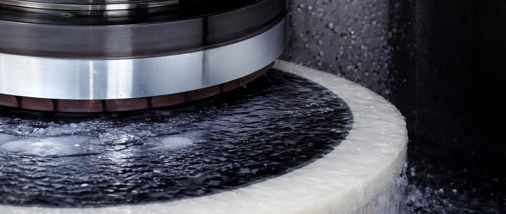
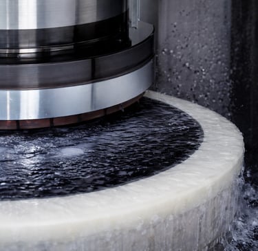
Coarse Grinding: Bulk Material Removal
Coarse grinding performs the majority of thickness reduction. Diamond-embedded grinding wheels remove silicon aggressively, often at material removal rates optimized for throughput rather than surface finish.
At this stage:
Subsurface damage is inevitable
Residual compressive and tensile stresses are introduced
Thickness variation (TTV) begins to form
The engineering goal is not damage elimination, but damage containment—ensuring that defects remain shallow enough to be removed or mitigated in later steps.
Fine Grinding: Damage Reduction and Thickness Control
Fine grinding transitions the process from removal to refinement. Finer grit wheels, lower feed rates, and tighter chuck control reduce surface roughness and limit further crack propagation.
Critical parameters include:
Wheel grit size and bond type
Chuck vacuum uniformity
Thermal load during grinding
This step largely determines final wafer thickness capability and downstream process margin.
Stress Relief and Surface Conditioning
Even after fine grinding, silicon retains residual stress and micro-damage. To address this, fabs may employ:
Stress relief grinding
Mechanical polishing
Wet etch or plasma etch damage removal
The choice depends on target thickness, device sensitivity, and cost constraints. Aggressive damage removal improves reliability but can exacerbate warpage if not carefully controlled.
Post-Backgrind Cleaning and Inspection
Grinding generates particles, slurry residue, and metallic contaminants. Post-backgrind cleaning must remove these without attacking exposed layers or inducing stiction-related damage.
Inspection typically focuses on:
Surface roughness
Edge chipping
Microcrack density
Wafer bow and warp
This is often the last chance to intercept latent defects before assembly.
Equipment Architecture and Process Limitations
Backgrinding tools are precision mechanical systems operating at the intersection of force, speed, and thermal control. Limitations arise not from any single subsystem, but from their interaction.
Chucking and Vacuum Control
Uniform chuck vacuum is critical. Non-uniform clamping leads to local bending during grinding, which amplifies subsurface damage and causes thickness non-uniformity.
As wafers thin:
Local stiffness drops sharply
Chuck flatness tolerance tightens
Warpage sensitivity increases
Grinding Wheel Wear and Conditioning
Grinding wheels are consumables, and their wear state directly affects removal rate, surface finish, and heat generation. Poor conditioning leads to glazing, increased friction, and thermally driven damage.
Thermal Management
Silicon may appear thermally robust, but thin wafers dissipate heat poorly. Localized temperature rise during grinding can induce slip lines, phase stress, and even device degradation near sensitive structures.
Failure Modes and Yield Risks in Wafer Backgrinding
Backgrinding-related yield loss often manifests downstream, making root-cause identification challenging.
Common failure modes include:
Subsurface microcracks that propagate during dicing
Edge chipping leading to die fracture
Excessive warpage causing pick-and-place or bonding failures
Delamination triggered during tape release
Latent reliability failures due to stress-induced defect activation
What makes these failures dangerous is their delayed visibility. A wafer may pass outgoing inspection yet fail catastrophically during assembly or reliability testing.
Wafer Backgrinding in Advanced Packaging Contexts
Advanced packaging amplifies every weakness in the backgrinding process.
Fan-Out and Panel-Level Packaging
Ultra-thin wafers are required to control mold flow and package warpage. Even minor thickness gradients translate into significant panel deformation.
TSV and 3D Integration
Backgrinding often serves as a TSV reveal step. Over-grinding risks copper extrusion or dielectric exposure; under-grinding compromises electrical continuity.
Power and RF Devices
Mechanical damage can alter carrier mobility, increase leakage, or degrade breakdown voltage. Backgrinding here becomes an electrical performance variable, not just a mechanical one.
Optimization Strategies and Process Trade-Offs
There is no universally “correct” backgrinding recipe. Optimization is always application-specific.
Key trade-offs include:
Throughput versus damage depth
Thickness capability versus warpage control
Aggressive thinning versus downstream yield margin
Successful fabs treat backgrinding as a co-engineered process, tightly coupled with dicing, assembly, and reliability requirements rather than an isolated cost center.
Backend Manufacturing Support with Silicon Craft Technologies
At the backend, wafer backgrinding rarely exists in isolation. Its success depends on how well it integrates with subsequent thinning-sensitive steps such as dicing, die attach, wire bonding, and advanced package build-up.
Silicon Craft Technologies supports wafer-level and package-level backend manufacturing with an engineering-driven approach that recognizes these interdependencies. Rather than treating backgrinding as a standalone operation, Si-Craft aligns thinning strategies with downstream assembly, reliability expectations, and package architecture requirements.
With capabilities spanning process development, prototyping, and low-to-medium volume production, Silicon Craft Technologies collaborates closely with customers to refine backend process windows, manage risk during scale-up, and adapt flows to evolving device and packaging demands. This integration-focused mindset is particularly critical as wafers become thinner, packages more complex, and tolerance for latent defects continues to shrink.
In modern semiconductor manufacturing, wafer backgrinding is no longer just about removing silicon—it is about preserving value. Supporting that balance between mechanical necessity and device integrity is where disciplined backend engineering makes the difference.