
Dicing Tape Selection
A technical deep dive into dicing tape selection, explaining how tape adhesion, stiffness, UV release behavior, and frame tension influence wafer singulation yield, die integrity, and long-term reliability in advanced semiconductor backend manufacturing.
Kiran
1/6/20265 min read
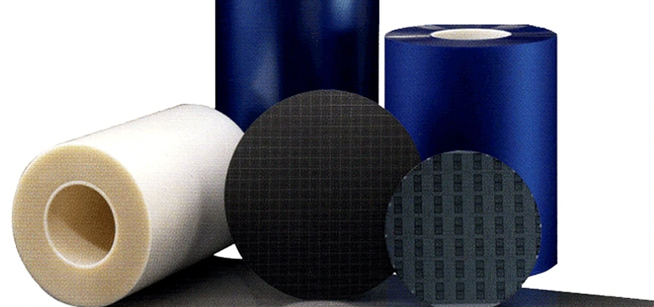
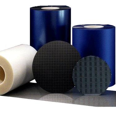
Rolls of semiconductor dicing and grinding tape used for wafer singulation, highlighting adhesive film materials that provide mechanical support and die retention during backend processing.
Dicing Tape Selection: A Critical Variable in Wafer Singulation Yield and Reliability
Introduction
In semiconductor backend manufacturing, dicing tape is often treated as an operational necessity rather than an engineering decision. Compared to tools, blades, lasers, or plasma systems, tape selection is frequently delegated to standard part numbers or legacy preferences. Yet as wafers become thinner, die edges more fragile, and backend structures extend closer to the scribe line, dicing tape has emerged as one of the most influential variables in singulation yield and downstream reliability.
Dicing tape is not passive. It actively constrains wafer motion, redistributes stress during cutting, controls die retention after singulation, and governs peel forces during pick-up. Poor tape selection can negate the benefits of an optimized dicing method, while correct tape selection can dramatically reduce chipping, cracking, die loss, and latent failures.
This article examines the functional role of dicing tape, explains how different tape properties influence singulation outcomes, and outlines how backend teams systematically select tape based on wafer thickness, dicing method, die size, and reliability targets.
The Functional Role of Dicing Tape
Mechanical Support During Singulation
The primary function of dicing tape is to support the wafer mechanically once it has been mounted on a frame. During dicing, the wafer is no longer supported uniformly from below; instead, the tape provides tensile support that constrains deflection and absorbs some of the stress introduced by cutting.
As wafers thin, this role becomes increasingly critical. Thin wafers rely heavily on tape stiffness and adhesion to prevent:
Excessive bowing
Vibration amplification
Localized bending near the cut
Inadequate support increases the likelihood of chipping, cracking, and catastrophic wafer breakage.
Key Dicing Tape Properties and Why They Matter
Adhesion Strength
Adhesion strength determines how firmly dies remain attached to the tape during and after dicing. This parameter affects two competing risks:
Low adhesion:
Die movement during dicing
Edge collisions between adjacent dies
Misalignment during pick-up
High adhesion:
Excessive peel force during die pick
Die cracking or corner breakage
Stress transfer into fragile backend structures
The optimal adhesion window is narrow and highly product-dependent.
Tape Elastic Modulus and Compliance
Tape stiffness controls how much the tape stretches and redistributes stress. Highly compliant tapes can absorb vibration but may allow excessive die movement. Stiffer tapes provide better positional stability but transmit more stress directly into the die.
This trade-off is especially important for:
Thin wafers
MEMS devices
Large dies with low fracture tolerance
Backend engineers must balance vibration damping against stress transmission when selecting tape modulus.
UV-Release Behavior
Many modern backend flows use UV-release dicing tapes, which reduce adhesion after UV exposure to facilitate die pick-up. While effective, UV tapes introduce additional variables:
UV dose uniformity
Exposure timing
Partial release gradients across the wafer
Non-uniform UV exposure can lead to inconsistent pick forces, increasing die breakage risk at the wafer edge or corners.
Surface Energy and Debris Interaction
Tape surface chemistry influences how dicing debris behaves. Some tapes attract particles, while others allow debris to migrate freely.
In advanced devices such as MEMS or WLCSP, particle retention near the die edge can:
Promote stiction
Cause electrical shorts
Interfere with solder joints
Tape selection therefore influences not only mechanical behavior but also cleanliness outcomes.
Tape Selection by Dicing Method
Blade Dicing
Blade dicing introduces the highest mechanical loads and vibration. For blade dicing, tape must:
Provide strong lateral support
Minimize die movement during cutting
Withstand coolant exposure
Stiffer tapes with moderate adhesion are typically preferred. Excessively soft tapes allow die flutter, increasing edge chipping.
Laser Dicing
Laser dicing reduces mechanical contact but introduces thermal gradients. Tape selection must account for:
Thermal expansion mismatch
Heat dissipation
Resistance to localized heating
In some laser flows, tapes with higher thermal stability and controlled compliance are used to prevent die drift during thermal cycling.
Plasma Dicing
Plasma dicing imposes minimal mechanical stress, shifting tape requirements toward:
Clean release behavior
Dimensional stability during long etch cycles
Compatibility with plasma environments
Because plasma dicing often uses very narrow kerfs, tape must precisely control die position to prevent edge contact after singulation.
Tape Selection for Thin and Ultra-Thin Wafers
Increased Dependence on Tape Properties
As wafer thickness decreases, tape becomes the primary structural support. For ultra-thin wafers:
Tape stiffness dominates system behavior
Adhesion uniformity becomes critical
Local defects in tape cause global failures
Tape variation that is negligible for thick wafers can be catastrophic for thin ones.
Interaction with Temporary Bonding
In flows that use temporary carriers, dicing tape interacts with the carrier system. Tape peel forces must be coordinated with debonding mechanics to avoid:
Die cracking
Residual adhesive contamination
Stress concentration during release
Tape and carrier selection must therefore be evaluated together rather than independently.
Die Size and Tape Behavior
Large Die vs Small Die
Large dies:
Experience higher peel forces
Are more sensitive to non-uniform adhesion
Store more elastic energy during tape stretch
Small dies:
Are more susceptible to loss or flipping
Require higher positional stability
Tolerate less die-to-die interaction
A tape that works well for one die size may be unsuitable for another, even on the same wafer.
Tape Stretch, Frame Tension, and Die Shift
Importance of Frame Tension Control
Tape is stretched over a metal frame during mounting. Frame tension determines:
In-plane stress in the tape
Die spacing uniformity after dicing
Pick-up force consistency
Over-tensioning increases peel force and crack risk. Under-tensioning allows die shift and collision.
Backend teams that treat frame tension as a controlled parameter—not a setup default—see significantly improved singulation consistency.
Tape Expansion During Pick-Up
Why Tape Expansion Is Risky
During die pick, some processes intentionally expand the tape to separate dies. While effective, expansion introduces tensile stress that can:
Open microcracks
Break die corners
Delaminate edge structures
This is especially dangerous for thin wafers and devices with edge-adjacent RDL or seal rings.
Cleanliness and Contamination Considerations
Tape adhesives can outgas, shed particles, or leave residue. These effects may not impact singulation yield but can cause:
Assembly defects
Poor solder wetting
Reliability degradation
Tape compatibility with downstream cleaning and assembly steps must be validated as part of tape selection.
Reliability Implications of Poor Tape Selection
Improper tape selection contributes to:
Latent die cracking
Solder joint fatigue
MEMS stiction failures
Moisture ingress via edge damage
Because these failures often occur far downstream, tape is frequently overlooked during root-cause analysis.
Backend Integration Perspective
Effective dicing tape selection requires system-level thinking rather than part substitution.
Silicon Craft Technologies approaches dicing tape selection as an integrated backend engineering decision, evaluating tape behavior alongside wafer thickness, dicing method, kerf width, and pick-up strategy. By treating tape as an active stress-management element rather than a consumable, Silicon Craft Technologies helps prevent tape-induced yield loss and latent reliability failures.
Qualification and Change Control
Tape changes should trigger:
Re-evaluation of dicing yield
Edge damage inspection
Pick force characterization
Reliability stress testing
Uncontrolled tape substitutions are a common source of unexplained yield drift.
Conclusion
Dicing tape selection is one of the most underestimated contributors to wafer singulation success. As backend processes push toward thinner wafers, narrower kerfs, and more fragile device architectures, tape behavior increasingly determines whether optimized dicing conditions translate into real yield and reliability gains.
Selecting the right tape requires:
Understanding mechanical and adhesive trade-offs
Matching tape properties to dicing method
Coordinating tape behavior with pick-up and assembly
Treating tape as an engineered component, not a consumable
In modern backend manufacturing, the wrong tape can undo months of process optimization—while the right tape can quietly enable it.