
Electroplating vs Evaporation
A detailed technical comparison of electroplating and evaporation in semiconductor backend manufacturing, exploring deposition mechanisms, thickness capability, process integration, cost trade-offs, and reliability impacts in advanced packaging.
Kiran
1/6/20265 min read
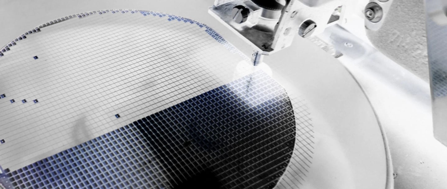
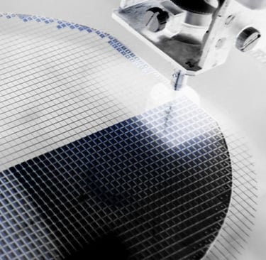
Automated tool performing metal deposition on a semiconductor wafer, illustrating electroplating used in backend wafer-level processing.
Electroplating vs Evaporation: Deposition Trade-Offs in Semiconductor Backend Manufacturing
Introduction
Thin-film metal deposition is a foundational step in semiconductor backend manufacturing, underpinning critical structures such as under-bump metallization (UBM), redistribution layers (RDL), seed layers, barrier films, and interconnect stacks. Among the many deposition techniques available, electroplating and physical vapor deposition (PVD) via evaporation represent two fundamentally different approaches—each with distinct process physics, equipment requirements, and manufacturing implications.
Although both methods are routinely described as “metal deposition,” they operate on entirely different principles. Electroplating is a wet, electrochemical, additive process driven by ionic transport and current density. Evaporation, by contrast, is a vacuum-based, line-of-sight physical process governed by vapor flux, surface kinetics, and chamber geometry.
Choosing between electroplating and evaporation is not a matter of preference but of engineering fit. The decision affects film thickness capability, uniformity, step coverage, throughput, cost, and ultimately device reliability. This article examines the two methods from a backend manufacturing perspective, focusing on how and why each technique is used, where it excels, and where its limitations define practical boundaries.
Fundamentals of Electroplating
Process Overview
Electroplating deposits metal by reducing dissolved metal ions from an electrolyte onto a conductive surface using an externally applied electric current. The wafer or substrate acts as the cathode, while an anode—either soluble or inert—completes the electrical circuit.
For semiconductor backend applications, electroplating is most commonly used to build thick copper layers, such as RDL traces, pillars, microbumps, and vias. Deposition rates are orders of magnitude higher than most vacuum methods, making electroplating the workhorse for structures requiring tens of microns of metal thickness.
Role of Seed Layers
Electroplating cannot occur on non-conductive surfaces. A thin, continuous seed layer—typically deposited by PVD—is required to initiate current flow. This seed layer defines the initial conductivity and strongly influences plating uniformity, adhesion, and grain structure.
The plating process therefore does not exist in isolation; it is tightly coupled to upstream deposition and surface preparation steps.
Thickness Control and Uniformity
Thickness in electroplating is controlled by current density, plating time, bath chemistry, and mass transport. While excellent uniformity is achievable, it requires careful management of edge effects, pattern density variation, and electrolyte flow.
Across-wafer uniformity is a function of both tool design and layout symmetry. Local pattern density variations can lead to thickness non-uniformity unless compensated by process tuning or dummy fill strategies.
Fundamentals of Evaporation (PVD)
Process Overview
Evaporation is a physical vapor deposition technique in which a solid metal source is heated—thermally or by electron beam—until atoms vaporize and travel through a high-vacuum environment before condensing on the wafer surface.
The process is fundamentally line-of-sight, meaning atoms travel in straight trajectories with limited scattering. This characteristic defines both the strengths and weaknesses of evaporation in backend manufacturing.
Film Characteristics
Evaporated films are typically dense, smooth, and have well-controlled thickness at the nanometer to sub-micron scale. Adhesion and film stress are strongly influenced by surface cleanliness, deposition rate, and substrate temperature.
Because evaporation occurs in vacuum without plasma, it is inherently gentle on underlying layers, making it suitable for delicate films and interfaces.
Thickness and Throughput Limitations
Evaporation is not practical for thick metal deposition. As thickness increases, deposition time grows linearly, throughput drops, and film stress becomes more difficult to manage. For this reason, evaporation is typically used for thin functional layers, such as adhesion layers, barrier metals, and seed films.
Deposition Thickness Regimes
One of the clearest distinctions between electroplating and evaporation is the thickness regime in which each operates effectively.
Electroplating excels in the micron to tens-of-microns range, where vacuum deposition would be prohibitively slow and expensive. Copper pillars, solder caps, and thick RDL traces are almost exclusively plated.
Evaporation dominates in the nanometer to low-micron range, where precision, cleanliness, and interface control are paramount. Adhesion layers like titanium, chromium, or tantalum, as well as noble metals such as gold, are commonly evaporated.
In practice, many backend stacks rely on both methods in sequence rather than choosing one exclusively.
Step Coverage and Topography Considerations
Electroplating Conformality
Electroplating is inherently conformal within patterned features because metal grows wherever current flows. In trenches or vias with adequate seed coverage, plating can achieve excellent sidewall and bottom fill, especially when combined with appropriate additives.
However, plating uniformity degrades if seed layers are discontinuous or resist profiles are poorly defined. Void formation and over-plating are common failure modes when process windows are not tightly controlled.
Evaporation Line-of-Sight Effects
Evaporation struggles with high-aspect-ratio features due to its directional nature. Shadowing effects can result in thin or missing coverage on sidewalls and feature bottoms.
This limitation makes evaporation poorly suited for filling vias or building thick topography but acceptable for blanket films on relatively flat surfaces.
Materials Compatibility
Electroplating Materials
Electroplating is most mature for copper, nickel, tin, silver, and certain alloys. Copper plating, in particular, has been optimized extensively for semiconductor applications due to its conductivity, electromigration resistance, and cost effectiveness.
Not all materials can be electroplated easily or reliably. Noble metals and refractory metals are generally challenging or impractical to plate with the precision required for advanced packaging.
Evaporation Materials
Evaporation supports a broad range of materials, including refractory metals, noble metals, and alloys that are difficult to plate. This versatility makes it ideal for adhesion layers, diffusion barriers, and specialized interfaces.
However, material utilization efficiency is low. A significant fraction of evaporated material deposits on chamber walls rather than the wafer, increasing cost for precious metals.
Process Integration and Yield Sensitivity
Electroplating Yield Drivers
Electroplating yield is sensitive to bath chemistry stability, contamination, current distribution, and resist integrity. Small excursions can manifest as thickness variation, roughness, or voids across many dies simultaneously.
Because plating is a wafer-level process, defects tend to be systematic rather than isolated, amplifying yield impact if not detected early.
Evaporation Yield Drivers
Evaporation yield is driven primarily by vacuum integrity, source stability, and surface cleanliness. While particle generation can be an issue, the absence of wet chemistry reduces some contamination risks.
Film defects in evaporation are often more localized, but poor adhesion or stress issues can have downstream reliability consequences.
Cost and Throughput Considerations
Electroplating offers high material efficiency and excellent throughput for thick films, making it cost-effective for volume production. Capital costs are relatively moderate, but operational costs include chemistry management and waste treatment.
Evaporation systems require high-vacuum infrastructure, have lower throughput for thick films, and suffer from poor material utilization. As a result, they are best reserved for thin layers where their precision justifies the cost.
From a cost-of-ownership perspective, each method is economically optimized for different roles rather than competing directly.
Reliability Implications
Film microstructure differs significantly between electroplated and evaporated metals. Electroplated copper tends to have larger grains and can exhibit anisotropy depending on process conditions, affecting electromigration and fatigue behavior.
Evaporated films are typically fine-grained and dense but can suffer from higher intrinsic stress if not carefully controlled.
Reliability performance therefore depends not only on the deposition method but on how it is integrated into the full stack and thermal history.
Decision Framework: When to Use Which
Electroplating is the method of choice when:
Thick metal layers are required
High aspect ratio features must be filled
Cost and throughput are critical
Copper is the primary conductor
Evaporation is preferred when:
Thin, precise films are needed
Adhesion and barrier layers are critical
Materials are difficult to plate
Surface damage must be minimized
In most advanced backend flows, the two methods are complementary rather than mutually exclusive.
Backend Manufacturing Support with Silicon Craft Technologies
Successfully integrating electroplating and evaporation into a reliable backend process flow requires more than selecting the right tool. It demands a deep understanding of how thin-film deposition interacts with lithography, thermal processing, mechanical stress, and downstream assembly behavior.
Silicon Craft Technologies supports these requirements through an engineering-driven backend manufacturing approach that spans thin-film deposition, wafer bumping, redistribution layer formation, and advanced packaging assembly. With hands-on experience in both electroplated and vacuum-deposited metallization stacks, Si-Craft helps customers align deposition strategy with functional requirements rather than defaulting to legacy choices.
During process development and prototyping, Silicon Craft Technologies works collaboratively to evaluate deposition trade-offs, identify yield-limiting mechanisms, and optimize integration between evaporation-based seed and barrier layers and electroplated functional metals. This capability is particularly valuable in low-to-medium volume production environments where flexibility, repeatability, and process understanding are critical.
By grounding deposition decisions in manufacturing realities and reliability expectations, Silicon Craft Technologies provides backend support that enables robust, scalable semiconductor packaging solutions—from early development through execution.