
Failure Mechanisms in Wafer Bumping
A comprehensive pillar guide explaining failure mechanisms in wafer bumping, covering material interactions, process-induced defects, reliability risks, and how wafer-level issues impact advanced semiconductor packaging performance.
Kiran
1/6/202612 min read
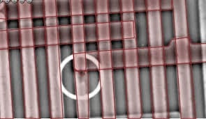

Optical micrograph showing fine RDL metal lines on a semiconductor wafer with a highlighted defect area.
Failure Mechanisms in Wafer Bumping: Root Causes, Detection, and Reliability Impact
Wafer bumping is a critical enabling process for flip-chip, wafer-level packaging (WLP), fan-out packaging, and advanced heterogeneous integration. While bumping technologies have matured significantly over the past two decades, failure mechanisms at the wafer bump level remain one of the most common root causes of package-level reliability issues.
Failures originating in wafer bumping are particularly costly because they are replicated across every die on a wafer. A single process deviation can result in thousands of latent defects that may only surface during downstream assembly, reliability testing, or even field operation. Understanding wafer bump failure mechanisms is therefore essential for yield protection, long-term reliability, and cost control.
This pillar article provides a comprehensive overview of failure mechanisms in wafer bumping, covering material interactions, process-induced defects, reliability degradation, inspection challenges, and mitigation strategies.
Overview of Wafer Bumping Technologies
Before examining failures, it is important to understand the common wafer bumping approaches where these mechanisms occur.
Typical wafer bumping technologies include:
Solder bumping (leaded and lead-free)
Copper pillar bumping
Microbump formation for advanced nodes
Stud bumping (gold or copper)
Wafer-level under-bump metallization (UBM) integration
Each technology introduces unique stresses and interfaces, but many failure mechanisms are shared across all bump types.
The Critical Role of Under-Bump Metallization
Under-bump metallization (UBM) forms the foundation of wafer bump reliability. The UBM stack typically includes:
An adhesion layer
A diffusion barrier
A solder-wettable or conductive top layer
Failures in wafer bumping often originate at UBM interfaces due to poor adhesion, improper thickness control, contamination, or intermetallic instability. Even when the bump itself appears mechanically intact, UBM degradation can cause electrical opens or latent failures.
Intermetallic Compound Formation and Growth
Intermetallic compound (IMC) formation is unavoidable in solder-based wafer bumping. IMCs form when solder reacts with UBM metals such as nickel or copper during reflow.
While controlled IMC formation is necessary for metallurgical bonding, excessive or uneven growth leads to failure.
Common IMC-related failure mechanisms include:
Brittle fracture at thick IMC layers
Kirkendall void formation due to unbalanced diffusion
IMC spalling during thermal cycling
Increased electrical resistance from IMC overgrowth
IMC growth accelerates with temperature, making this a major concern for automotive, industrial, and high-power applications.
Solder Void Formation
Voids within solder bumps are one of the most frequently observed wafer bump defects. These voids may form during solder deposition, reflow, or solidification.
Primary causes include:
Entrapped flux residues
Outgassing during reflow
Inadequate wetting of the UBM
Poor reflow profile control
Voids reduce the effective load-bearing area of the bump and increase current density, accelerating electromigration and thermal fatigue. Large voids or clustered voids can cause early mechanical failure during thermal cycling.
Non-Uniform Bump Height and Coplanarity Issues
Bump height uniformity is essential for reliable die attach and assembly. Non-uniform bump height can result from:
Electroplating non-uniformity
Photoresist thickness variation
Uneven reflow conditions
Wafer warpage during bump formation
Poor coplanarity leads to open joints during flip-chip attach, head-in-pillow defects, or excessive stress on individual bumps. These failures may not be detected at wafer level but emerge during assembly.
UBM Delamination and Adhesion Failure
Adhesion failures between UBM layers or between UBM and the pad metallization are a major reliability risk. Delamination may be partial or complete and is often difficult to detect without destructive analysis.
Root causes include:
Surface contamination prior to UBM deposition
Incompatible pad metallurgy
Insufficient adhesion layer thickness
Thermal stress from CTE mismatch
UBM delamination typically results in electrical opens, intermittent connections, or early life failures during temperature cycling.
Electromigration in Wafer Bumps
As bump pitch shrinks and current density increases, electromigration becomes a dominant failure mechanism. Electromigration occurs when metal atoms migrate under high current density, forming voids and hillocks.
Wafer bump electromigration is influenced by:
Bump diameter and geometry
Solder alloy composition
UBM barrier effectiveness
Operating temperature and duty cycle
Electromigration damage often initiates at the UBM interface and progresses invisibly until catastrophic failure occurs.
Copper Pillar-Specific Failure Mechanisms
Copper pillar bumping introduces additional failure modes compared to solder bumps.
Common copper pillar failures include:
Copper pillar cracking due to stress concentration
Interface failure between copper pillar and solder cap
Barrier layer breakdown allowing copper diffusion
Fatigue cracking at the pillar-to-die interface
Copper pillars offer superior current carrying capability, but they require tighter process control and material compatibility to avoid reliability degradation.
Cracking and Mechanical Fatigue
Mechanical fatigue is driven by thermal cycling, power cycling, and mechanical loading. Repeated expansion and contraction cause stress accumulation at bump interfaces.
Cracks may form:
Within the solder bump
At the IMC layer
At the UBM interface
At the die or substrate interface
Crack propagation is often slow and difficult to detect early, making fatigue one of the most dangerous latent failure mechanisms.
Warpage-Induced Bump Damage
Wafer and package warpage can cause bump deformation during processing or assembly. Warpage sources include:
Thick metal layers
Asymmetric RDL stacks
Mold compound shrinkage
Temperature gradients
Excessive warpage leads to bump shear stress, misalignment, and localized plastic deformation, increasing the risk of early failure.
Flux and Residue-Related Failures
Residual flux trapped near wafer bumps can lead to corrosion, leakage current, and long-term reliability issues. Inadequate cleaning after bumping or reflow can leave ionic contaminants.
Over time, moisture absorption accelerates electrochemical migration, particularly in fine-pitch bump arrays.
Oxidation and Surface Contamination
Oxidation of solder or UBM surfaces reduces wettability and bond strength. Oxide formation can occur during storage, handling, or insufficiently controlled reflow atmospheres.
Contamination sources include:
Organic residues
Particulates
Moisture exposure
Even trace contamination can significantly degrade bump integrity at advanced nodes.
Microbump Scaling Challenges
As microbump pitch drops below 40 µm, failure mechanisms become more severe and less forgiving. Smaller bumps experience:
Higher current density
Reduced mechanical compliance
Increased sensitivity to process variation
Microbump failures often result from a combination of electromigration, IMC brittleness, and mechanical fatigue.
Inspection and Detection Challenges
Many wafer bump failures are difficult to detect using non-destructive inspection methods. Common inspection techniques include:
Optical inspection
X-ray imaging
Scanning acoustic microscopy
Electrical continuity testing
However, defects such as micro-voids, early IMC degradation, or interfacial delamination often require destructive cross-section analysis for confirmation.
Reliability Testing and Failure Acceleration
Reliability testing accelerates wafer bump failure mechanisms to predict long-term performance. Common tests include:
Thermal cycling
Thermal shock
High-temperature storage
Power cycling
Humidity bias testing
Failure analysis from these tests provides critical feedback for bump process optimization.
Process Control as a Failure Mitigation Strategy
Most wafer bump failures are not design issues but process control issues. Tight control of:
UBM deposition
Plating uniformity
Reflow profile
Cleaning steps
Environmental conditions
significantly reduces defect rates and improves reliability margins.
Design-for-Reliability Considerations
Effective wafer bump reliability starts at the design stage. Design considerations include:
Appropriate bump size and pitch
Balanced RDL thickness
Proper UBM material selection
Redundant power and ground bumps
Designing with process capability in mind reduces sensitivity to variation.
Thermo-Mechanical Mismatch Between Die, Bump, and Substrate
One of the most persistent contributors to wafer bump failure is thermo-mechanical mismatch between the silicon die, solder bump, and organic or ceramic substrate. Each material expands and contracts at different rates when exposed to temperature changes, creating cyclic stress at bump interfaces.
Silicon has a relatively low coefficient of thermal expansion (CTE), while solder alloys and substrates expand more aggressively. During thermal cycling, this mismatch generates shear stress concentrated at the bump–UBM interface and within the solder matrix itself. Over time, this stress accumulation leads to fatigue damage, microcrack initiation, and eventual joint failure.
This issue becomes more pronounced as bump pitch decreases and bump height is reduced, limiting the ability of the solder to absorb mechanical strain through plastic deformation.
Pad Metallurgy Compatibility Failures
Wafer bump reliability depends heavily on compatibility between the die pad metallurgy and the UBM stack. Aluminum, copper, and alloyed pad surfaces react differently with adhesion and barrier layers.
Failure mechanisms associated with poor pad compatibility include:
Weak adhesion at the pad–UBM interface
Localized corrosion at dissimilar metal boundaries
Accelerated intermetallic formation
Electrical opens due to interface separation
In advanced nodes, pad surface treatments and passivation openings introduce additional complexity. Even small variations in pad cleanliness or oxide thickness can result in widespread bump adhesion failures across an entire wafer.
Barrier Layer Degradation and Diffusion Failures
Diffusion barrier layers are designed to prevent uncontrolled metal migration between solder and underlying metallization. When barrier layers are too thin, damaged, or poorly deposited, diffusion-related failures become inevitable.
Common diffusion-related failure mechanisms include:
Copper diffusion into solder causing embrittlement
Nickel depletion leading to weak solder interfaces
Barrier cracking under thermal stress
Localized corrosion pathways forming at diffusion sites
Barrier degradation is often a latent failure mechanism, becoming apparent only after extended thermal exposure or high-temperature storage testing.
High-Temperature Storage-Induced Failures
High-temperature storage (HTS) testing is particularly effective at revealing wafer bump weaknesses related to material stability. Prolonged exposure to elevated temperatures accelerates intermetallic growth, diffusion, and oxidation.
Failure mechanisms observed after HTS include:
Excessive IMC thickening
Loss of solder ductility
UBM thinning or depletion
Increased electrical resistance
Devices intended for automotive, industrial, or power electronics applications are especially vulnerable to HTS-related degradation if bump metallurgy is not properly optimized.
Moisture Ingress and Corrosion-Driven Failures
Moisture exposure introduces another class of wafer bump failure mechanisms. Moisture can penetrate microvoids, cracks, or weak interfaces, enabling corrosion and electrochemical migration.
Corrosion-driven failures are often associated with:
Residual flux contamination
Ionic residues from incomplete cleaning
Poor encapsulation or passivation integrity
In fine-pitch bump arrays, moisture-induced failures can propagate rapidly due to short inter-bump spacing, resulting in leakage current, short circuits, or sudden electrical failure.
Head-in-Pillow Defects Originating at Wafer Level
Although often attributed to assembly, head-in-pillow defects can originate from wafer bumping issues. Oxidized or contaminated bump surfaces may fail to wet properly during reflow, even when placement is correct.
Wafer-level contributors to head-in-pillow include:
Surface oxidation during storage
Non-uniform bump height
Improper solder alloy selection
Excessive IMC formation prior to assembly
Because these defects manifest during board or substrate attach, their true origin is frequently misdiagnosed.
Residual Stress Accumulation During Bump Formation
Residual stress is introduced at multiple stages of wafer bumping, including UBM deposition, electroplating, and reflow. These stresses may not immediately cause failure but weaken the bump structure over time.
Sources of residual stress include:
Plating stress from electrochemical deposition
Thermal gradients during reflow
CTE mismatch within the UBM stack
Asymmetric metal layer thickness
Residual stress reduces the margin for additional stress during operation, accelerating fatigue-related failures.
Fine-Pitch Routing Density Effects on Bump Reliability
As routing density increases, bumps are placed closer together and supported by thinner dielectric layers. This creates a mechanically constrained environment where stress cannot dissipate easily.
High-density layouts increase susceptibility to:
Crack propagation between adjacent bumps
Stress coupling across the bump array
Localized warpage amplification
Electrical shorting due to metal migration
Failure mechanisms in dense arrays tend to be systemic rather than isolated, leading to rapid yield loss once thresholds are exceeded.
Yield Amplification Effect of Wafer-Level Defects
One of the most dangerous aspects of wafer bump failure mechanisms is yield amplification. A single process defect affects every die on the wafer simultaneously.
For example:
A plating chemistry imbalance affects all bumps
A UBM adhesion issue repeats across the wafer
A reflow profile error impacts every solder joint
This amplification effect makes wafer bumping one of the highest-risk backend processes from a yield perspective, demanding exceptional process discipline.
Statistical Process Drift and Latent Failures
Wafer bump failures are often not caused by catastrophic process errors but by gradual statistical drift. Small shifts in thickness, composition, or temperature can accumulate over time.
Without tight statistical process control (SPC), drift-related failures may go unnoticed until field returns occur. These failures are difficult to trace back to root cause without historical process data.
Failure Propagation into Package-Level Defects
Wafer bump defects rarely remain isolated at the bump level. They propagate into higher-level failures such as:
Die attach failures
Substrate cracking
Mold compound delamination
System-level electrical instability
Because wafer bumping sits at the foundation of the package stack, its failure mechanisms influence every downstream process.
Advanced Nodes and Future Scaling Risks
As industry moves toward sub-20 µm pitch microbumps and hybrid bonding, traditional failure mechanisms intensify rather than disappear. Reduced bump volume limits stress absorption, while higher current density accelerates degradation.
Future risks include:
Ultra-thin IMC brittleness
Increased electromigration sensitivity
Reduced inspection resolution
Tighter process windows with less tolerance for variation
Understanding today’s wafer bump failure mechanisms is essential preparation for future packaging technologies.
Closing Perspective on Failure Mechanisms in Wafer Bumping
Wafer bumping failure mechanisms are rarely the result of a single factor. Instead, they emerge from complex interactions between materials, processes, design decisions, and operating conditions.
Long-term reliability requires:
Robust UBM and bump design
Tight process control
Comprehensive inspection
Aggressive reliability qualification
Close collaboration between design and backend manufacturing teams
As wafer bumping continues to evolve, failure prevention will depend not on incremental fixes but on system-level understanding and optimization.
Backend Manufacturing Support with Silicon Craft Technologies
Addressing wafer bump failure mechanisms requires close integration between design, process development, and reliability validation. Silicon Craft Technologies provides backend manufacturing support focused on wafer bumping, advanced packaging, and reliability engineering.
Silicon Craft Technologies works with customers to identify root causes of bump failures, optimize UBM and bump processes, and implement robust inspection and qualification strategies. Their backend expertise supports both early development and high-volume manufacturing environments.
Conclusion
Failure mechanisms in wafer bumping are complex, interrelated, and often latent. Small defects at the wafer level can propagate into catastrophic package failures if not properly understood and controlled.
By combining sound design practices, robust process control, and comprehensive reliability testing, manufacturers can significantly reduce wafer bump failure risk. As bump pitches continue to shrink and packaging complexity increases, a deep understanding of these failure mechanisms becomes not just beneficial—but essential.