
How Wafer Warpage Impacts Assembly Yield—and How to Control It
Discover how wafer warpage affects assembly yield and learn practical methods to control distortion, reduce defects, and improve semiconductor manufacturing efficiency.
1/5/202612 min read
How Wafer Warpage Impacts Assembly Yield—and How to Control It
Wafer warpage has transitioned from a secondary mechanical concern into a primary yield limiter in advanced semiconductor assembly. As device architectures evolve toward thinner substrates, higher interconnect density, and heterogeneous integration, the mechanical behavior of wafers increasingly dictates what is manufacturable at scale. In many modern backend flows, warpage is no longer a marginal specification checked at the end of processing—it is a dominant constraint that influences equipment selection, process windows, and long-term reliability.
This article provides a detailed, engineering-focused analysis of wafer warpage: how it originates, how it propagates through backend manufacturing, how it directly impacts assembly yield, and which control strategies are effective in production environments. Rather than treating warpage as a standalone defect, the discussion frames it as a system-level outcome shaped by materials, process sequencing, and thermal-mechanical interactions across the entire wafer lifecycle.
Understanding Wafer Warpage in Advanced Semiconductor Manufacturing
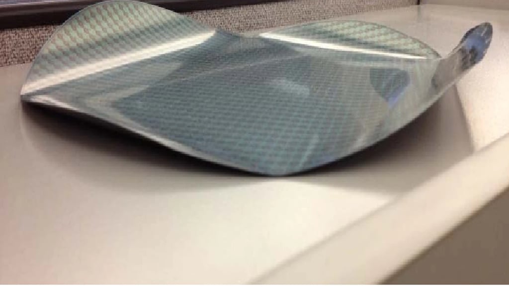
Wafer warpage refers to out-of-plane deformation of a wafer caused by residual stress, thermal mismatch, or non-uniform material removal. It is commonly described using metrics such as bow and warp, but these measurements are only surface indicators of deeper mechanical imbalance within the wafer stack.
Historically, warpage was largely mitigated by wafer thickness. Front-end wafers remained mechanically stiff enough that stress gradients introduced by thin films or thermal cycles had limited macroscopic effect. As backend processes demanded aggressive thinning—often to well below 100 µm—this inherent stiffness was removed. The wafer’s ability to self-balance internal stress collapsed, allowing even modest asymmetries to produce significant curvature.
In advanced packaging, where assembly tolerances are measured in microns and interconnect pitches continue to shrink, this curvature directly interferes with tool assumptions. Assembly equipment, inspection systems, and handling automation are fundamentally designed around the expectation of near-planar substrates. Warpage violates that assumption.
Fundamental Mechanical Drivers of Wafer Warpage
Wafer warpage does not arise from a single process step. It is the cumulative result of mechanical and thermal history, with multiple contributors that interact in non-linear ways.
Residual Stress in Thin Films
Thin films deposited during backend processing—dielectrics, barrier layers, redistribution metals, and passivation stacks—carry intrinsic stress determined by their deposition conditions. This stress may be tensile or compressive and can vary with parameters such as temperature, plasma power, pressure, and film thickness.
When these films are applied asymmetrically or in unbalanced thicknesses, they create bending moments across the wafer. At full wafer thickness, these moments may be partially absorbed by bulk silicon. As the wafer is thinned, the same stress produces exponentially greater curvature.
Thermal Expansion Mismatch
Every material in the wafer stack expands and contracts with temperature, but not at the same rate. Silicon, metals, polymers, and dielectrics all have distinct coefficients of thermal expansion. During thermal excursions—curing, annealing, reflow, or even prolonged tool dwell—these differences generate interfacial stress.
Critically, warpage is often driven not by peak temperature alone, but by thermal gradients and ramp rates. Rapid heating or cooling can freeze stress into the structure before relaxation mechanisms occur, locking in curvature that persists through assembly.
Wafer Thinning-Induced Stress Redistribution
Backgrinding and polishing remove silicon that previously acted as a mechanical counterbalance. This exposes latent stress that may have accumulated earlier in the flow. In many cases, wafers appear relatively flat prior to thinning, only to exhibit severe warpage afterward.
Non-uniform material removal, local heating during grinding, or inadequate support can exacerbate this effect. Once thinning is complete, options for stress redistribution are limited.
Temporary Bonding and Debonding Effects
Temporary wafer bonding is widely used to enable thinning and backside processing. While essential, it introduces additional materials and interfaces that influence stress evolution. Bonding adhesives, carrier substrates, and debonding forces can all contribute to residual curvature if their properties are not well matched to the process flow.
Debonding is particularly critical. Mechanical peeling, thermal release, or laser-assisted separation can introduce non-uniform forces that permanently deform the device wafer.
How Wafer Warpage Directly Impacts Assembly Yield
The impact of wafer warpage on assembly yield is multifaceted. Some effects are immediately visible as placement failures, while others manifest as latent reliability risks that escape early detection.
Die Attach Accuracy and Planarity
Die attach processes assume a consistent z-height across the wafer or panel. Warpage disrupts this assumption, causing variations in contact force during placement. In extreme cases, this leads to tilted dies, uneven adhesive thickness, or incomplete bonding.
Even moderate warpage can reduce process margin, forcing tighter tool tuning and increasing sensitivity to minor variations in adhesive viscosity or placement speed.
Flip-Chip and Solder Joint Integrity
In flip-chip assembly, planarity is critical for uniform solder joint formation. Warped wafers create non-uniform gaps between mating surfaces, leading to uneven solder collapse, head-in-pillow defects, or incomplete wetting.
These issues may not cause immediate electrical failures, but they significantly reduce mechanical fatigue life under thermal cycling. From a yield perspective, this translates into higher field failure rates and reduced product lifetime.
Handling, Chucking, and Automation Losses
Automated handling systems rely on vacuum chucks, edge grippers, and alignment stages that assume predictable wafer geometry. Excessive warpage reduces chucking efficiency, increases the risk of wafer slip, and triggers tool alarms.
Even when wafers remain processable, throughput suffers. Increased tool downtime, manual intervention, and rework all contribute to effective yield loss.
Inspection and Metrology Degradation
Warped wafers complicate optical inspection by introducing focus variation across the field of view. Metrology tools may struggle to maintain measurement accuracy, particularly for overlay and critical dimension control.
As a result, defects may be missed, misclassified, or detected too late in the flow to allow corrective action.
Warpage Metrics and Measurement Challenges
Measuring wafer warpage is straightforward in principle but complex in practice. Different metrics capture different aspects of deformation, and not all are equally relevant to assembly risk.
Bow, Warp, and Shape Complexity
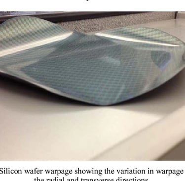
Bow typically measures the deviation of the wafer center from a reference plane, while warp captures the maximum peak-to-valley deviation across the entire surface. Localized curvature, however, can be just as damaging as global deformation.
Two wafers with identical bow values may behave very differently in assembly if one exhibits localized saddle-shaped distortion while the other has smooth, symmetric curvature.
Temperature-Dependent Warpage Behavior
Warpage is not static. Many wafers exhibit temperature-dependent behavior, appearing within specification at room temperature but exceeding limits at elevated temperatures encountered during assembly or reflow.
Measuring warpage across relevant temperature ranges provides more actionable insight than single-point measurements.
In-Process Metrology Strategy
End-of-line warpage measurements offer limited value if corrective options are exhausted. In-process monitoring—after thinning, after major deposition steps, or after debonding—enables earlier intervention and reduces the risk of scrapping high-value wafers.
Assembly-Flow-Specific Sensitivity to Warpage
Different assembly technologies exhibit different tolerance levels for warpage, but none are immune.
Wire Bond Assembly
Wire bonding is sensitive to substrate planarity because warpage affects bond pad height and loop geometry. Excessive curvature can lead to inconsistent loop heights, bond lift, or heel cracking, particularly as pitch decreases.
Flip-Chip Assembly
Flip-chip processes are among the most warpage-sensitive. Fine-pitch solder joints require uniform collapse and consistent standoff height. Warpage directly undermines both, increasing defect rates and reducing reliability margins.
Fan-Out Wafer-Level Packaging
In fan-out flows, warpage complicates mold flow, redistribution layer lithography, and singulation. Warped wafers are more prone to molding voids, lithography focus errors, and mechanical damage during dicing.
Process-Level Strategies for Controlling Wafer Warpage
Effective warpage control requires coordinated action across materials, processes, and equipment. Isolated fixes rarely deliver sustainable results.
Symmetric Stack Design
Where possible, backend layer stacks should be designed to balance stress around the wafer midplane. This may involve adjusting metal and dielectric thicknesses or sequencing depositions to counteract stress accumulation.
Perfect symmetry is rarely achievable, but even partial balancing can significantly reduce curvature.
Thin-Film Stress Engineering
Many thin films allow stress tuning through deposition parameters. Selecting low-stress recipes and maintaining tight process control reduces cumulative distortion. Long-term stability must also be considered, as stress relaxation over time can reintroduce warpage.
Thermal Budget Management
Reducing unnecessary thermal excursions and controlling ramp rates limits stress buildup. In some cases, replacing high-temperature steps with lower-temperature alternatives provides measurable warpage reduction without compromising electrical performance.
Temporary Carrier Optimization
Carrier material selection, bonding layer properties, and debonding methods should be evaluated not only for compatibility, but for their impact on residual stress. Carrier mismatch and aggressive debonding are common root causes of late-stage warpage.
Assembly Tool Adaptation
When upstream warpage cannot be fully eliminated, assembly tools may be adapted through compliant chucks, adaptive vacuum zoning, or dynamic height control. These measures extend process windows but should be viewed as secondary mitigation rather than primary solutions.
Designing for Warpage Control Early in Development
The most effective warpage mitigation occurs early, during product and process definition. Once materials and flows are locked, options become increasingly constrained.
Integrating mechanical considerations into design-for-manufacturing reviews, simulating stress evolution, and validating assumptions through early prototyping significantly reduce downstream yield risk.
Mechanical Stress Modeling and Its Role in Predicting Warpage
As wafer warpage becomes a dominant assembly constraint, empirical observation alone is no longer sufficient for effective control. Mechanical stress modeling has therefore become an increasingly important tool in backend process development. While full predictive accuracy remains challenging, modeling provides valuable directional insight into how materials, layer stacks, and thermal histories interact.
At its core, warpage modeling treats the wafer as a multilayer composite structure. Each layer is defined by thickness, elastic modulus, Poisson’s ratio, intrinsic stress, and coefficient of thermal expansion. By solving force and moment equilibrium across the stack, engineers can estimate curvature under different thermal conditions.
The primary value of modeling is not absolute prediction, but sensitivity analysis. It allows teams to identify which layers dominate bending behavior and which process steps contribute most strongly to curvature. For example, simulations often reveal that a relatively thin polymer or passivation layer can outweigh thicker metal layers due to its thermal expansion mismatch and viscoelastic behavior.
Modeling also highlights why warpage control must be addressed early. Once the stack is defined and material choices are locked, degrees of freedom collapse. Late-stage fixes tend to be compensatory rather than corrective, increasing cost and complexity without fully restoring margin.
Viscoelastic Effects and Time-Dependent Warpage
A critical but often underestimated contributor to wafer warpage is time-dependent material behavior. Many backend materials—particularly polymers, adhesives, and certain low-k dielectrics—exhibit viscoelastic properties. Their stress state evolves not only with temperature, but with time under load.
This means that warpage can change between process steps, during tool queue time, or even while wafers sit in storage. A wafer that meets flatness requirements immediately after debonding may drift out of specification hours or days later as stresses relax or redistribute.
From an assembly standpoint, this introduces scheduling sensitivity. Wafers processed under identical conditions may behave differently depending on how long they remain at ambient or elevated temperature before assembly. Without accounting for viscoelastic effects, yield loss may appear random or intermittent.
Mitigation strategies include controlling queue times, standardizing thermal histories, and selecting materials with stable long-term mechanical behavior. In high-volume environments, even small reductions in variability translate into meaningful yield improvements.
Warpage-Induced Failure Modes Beyond Immediate Yield Loss
While many warpage-related issues manifest during assembly, others remain latent until reliability testing or field operation. These failure modes are particularly costly because they bypass early screening.
One common example is interconnect fatigue acceleration. Warpage-induced non-uniform solder joint geometry concentrates strain during thermal cycling. Over time, this accelerates crack initiation and propagation, reducing mean time to failure.
Another subtle mechanism is die cracking or delamination. Curved substrates impose bending stress on mounted dies, especially during temperature excursions. Even if initial assembly appears successful, repeated cycling can cause interfacial separation or microcracking that eventually leads to electrical failure.
These risks underscore why warpage should be treated as a reliability parameter, not just an assembly metric. Yield metrics that focus solely on immediate pass/fail outcomes may underestimate the long-term cost of inadequate warpage control.
Panel-Level and Large-Format Assembly Considerations
As the industry explores larger substrates and panel-level packaging, warpage challenges scale nonlinearly. Increasing substrate size does not merely magnify curvature—it amplifies its impact on tool compatibility and process uniformity.
Large panels are inherently more flexible, making them more sensitive to residual stress. Gravity-induced sag, handling-induced distortion, and thermal gradients across the panel surface all interact with intrinsic warpage.
Assembly tools designed for wafers often struggle to accommodate these effects. Vacuum zoning becomes more complex, alignment tolerances tighten, and the margin for error shrinks. In this context, warpage control becomes a prerequisite for panel-level scalability.
Process flows that appear stable at wafer scale may fail entirely when translated to panels unless mechanical behavior is re-evaluated holistically.
Trade-Offs Between Warpage Control and Other Process Objectives
Warpage optimization rarely occurs in isolation. Measures taken to reduce curvature often interact with electrical, thermal, or cost objectives, creating trade-offs that must be managed deliberately.
For example, increasing dielectric thickness may reduce stress imbalance but degrade electrical performance. Lowering thermal budgets may improve flatness but limit material options or throughput. Adding compensating layers may restore symmetry but introduce additional interfaces and reliability risks.
Effective warpage control therefore requires prioritization. Not all curvature is equally harmful, and not all flatness improvements justify their cost. The goal is not zero warpage, but acceptable warpage within the constraints of assembly and reliability requirements.
This perspective shifts the discussion from specification chasing to system optimization.
Cross-Functional Ownership of Warpage Control
One of the most persistent challenges in managing wafer warpage is organizational rather than technical. Responsibility for warpage often falls between teams: design defines materials, process engineering defines flows, and assembly absorbs the consequences.
Without clear ownership, warpage issues are addressed reactively. Yield loss triggers investigation, but corrective actions are limited because upstream decisions are already fixed.
Leading organizations address this by assigning explicit cross-functional ownership for mechanical integrity. Warpage targets are defined early, reviewed at major process milestones, and validated with both modeling and empirical data. This approach aligns incentives and reduces late-stage surprises.
Warpage Control as an Enabler of Future Integration
Looking forward, wafer warpage will become even more critical as integration density increases and substrates continue to thin. Technologies such as chiplets, hybrid bonding, and advanced fan-out architectures all impose tighter planarity requirements.
In this context, warpage control is not merely defensive—it is enabling. Processes that cannot maintain mechanical stability will be excluded from next-generation integration schemes, regardless of their electrical merits.
Organizations that develop robust, transferable warpage control methodologies today will be better positioned to adopt future architectures without disruptive redesigns.
Quantifying Acceptable Warpage: Specification Limits vs. Process Reality
One of the persistent challenges in managing wafer warpage is the disconnect between formal specifications and actual process capability. Flatness limits are often defined conservatively, based on tool vendor recommendations or legacy requirements, without fully accounting for how warpage interacts with a specific assembly flow.
In practice, not all warpage is equally harmful. Smooth, axisymmetric bow may be tolerated by some assembly tools, while localized saddle-shaped distortion can cause failures even when overall warp values appear acceptable. This makes single-number specifications insufficient as standalone acceptance criteria.
A more effective approach is to correlate warpage measurements with concrete assembly outcomes. By mapping defect rates, placement errors, or solder joint anomalies against measured warpage profiles, engineers can establish process-specific control limits rather than relying solely on generic specifications.
This data-driven alignment allows tighter control where it matters most, while avoiding unnecessary scrap of wafers that are mechanically acceptable for a given flow.
Tool-Induced Warpage Amplification During Assembly
While wafer warpage is often treated as an upstream issue, assembly tools themselves can amplify existing curvature. Vacuum chucks, clamps, and thermal stages impose boundary conditions that may force warped wafers into unnatural shapes during processing.
For example, aggressive vacuum chucking can locally flatten a curved wafer, storing elastic energy that is released once the wafer is unclamped. This snap-back effect can exacerbate distortion during subsequent handling or reflow, increasing variability across lots.
Thermal gradients within assembly tools also play a role. Non-uniform heating across the wafer surface can temporarily increase curvature during critical process steps, even if room-temperature warpage appears controlled.
Understanding these interactions is essential. In some cases, modifying chuck design, zoning, or thermal uniformity yields greater benefit than further upstream stress reduction.
Lot-to-Lot and Within-Lot Warpage Variability
Even when average warpage is well controlled, variability can still undermine yield. Lot-to-lot variation often arises from subtle differences in material batches, deposition conditions, or thermal histories that fall within nominal specifications but alter stress balance.
Within-lot variability is equally problematic. Edge wafers may experience different thermal exposure than center wafers, while small thickness variations introduced during grinding can translate into measurable curvature differences after thinning.
From a yield standpoint, variability is often more damaging than absolute magnitude. Assembly tools can sometimes be tuned for a known curvature profile, but inconsistent behavior across wafers increases setup complexity and defect risk.
Reducing variability requires tight control of upstream processes and consistent handling protocols, particularly for thin and bonded wafers.
Warpage Control in Low-Volume and Prototyping Environments
Warpage challenges are often more pronounced in low-volume or development settings, where processes are still being optimized and material combinations change frequently. Limited statistical data makes it harder to distinguish systematic issues from random variation.
In these environments, warpage control relies heavily on engineering judgment and rapid feedback loops. Frequent measurement, visual inspection, and short iteration cycles are critical to preventing the accumulation of hidden stress issues.
Prototyping flows that ignore warpage until assembly frequently encounter late-stage surprises that delay development schedules. Incorporating warpage awareness early—even before formal specifications are established—reduces rework and accelerates learning.
Economic Impact of Warpage-Driven Yield Loss
Beyond technical consequences, wafer warpage carries significant economic implications. Yield loss attributed to warpage is often indirect, appearing as increased rework, longer cycle times, or reduced equipment utilization rather than immediate scrap.
Dropped wafers, tool downtime, and manual intervention erode throughput and inflate cost per unit. Latent reliability failures further amplify cost through warranty exposure and reputational risk.
When evaluated holistically, investments in warpage control—whether through materials optimization, metrology, or process refinement—often deliver strong returns by stabilizing downstream operations.
Warpage as a Design-for-Manufacturing Constraint
As semiconductor manufacturing continues to integrate mechanical, electrical, and thermal considerations, warpage must be treated as a core design-for-manufacturing parameter. Decisions about layer stacks, materials, and thermal budgets should explicitly account for their mechanical consequences.
Design teams that incorporate warpage considerations early reduce dependency on downstream mitigation and improve overall manufacturability. This shift transforms warpage from a recurring problem into a managed constraint.
Backend Manufacturing Support with Silicon Craft Technologies
Managing wafer warpage requires an integrated understanding of materials, process sequencing, and assembly constraints. Silicon Craft Technologies applies an engineering-driven approach to backend semiconductor manufacturing, supporting wafer-level and package-level processes where mechanical behavior directly influences yield.
By working closely with customers during process development, prototyping, and low-to-medium volume production, Si-Craft helps identify where warpage originates and how it propagates through thinning, processing, and assembly. This collaborative methodology enables practical control strategies aligned with manufacturability, reliability, and yield objectives.
Rather than treating warpage as an isolated metric, Silicon Craft Technologies incorporates mechanical considerations into backend process design, ensuring that assembly yield remains predictable as device architectures and integration complexity continue to advance.
“Close-up of a temporary wafer bonding tool clamping a silicon wafer on a carrier substrate for backend semiconductor manufacturing”