
Introduction to Wafer Backgrinding: Processes, Materials, and Techniques for Modern Semiconductor Manufacturing
Discover how wafer backgrinding enables today’s ultra-thin, high-performance semiconductor devices. This article explains the fundamentals of wafer thinning, the differences between grinding and lapping, and how material type and wafer size influence the choice of process. From small-diameter compound wafers to large 300 mm silicon substrates, learn how each method maintains integrity, minimizes damage, and prepares wafers for advanced packaging and 3D integration. Perfect for engineers, technologists, and anyone seeking a clear, detailed introduction to modern wafer backgrinding techniques.
10/2/20253 min read
As semiconductor devices continue shrinking while demanding higher performance, the need for ultra-thin wafers has become fundamental to advanced packaging, high-density memory, mobile SoCs, CMOS image sensors, and multi-layer stacking technologies. Wafer backgrinding—also known as wafer thinning—plays a central role in enabling these form factors. By reducing wafer thickness from its as-processed state (typically 600–750 µm) to as thin as 50–75 µm—and in some cases well below 30 µm—the process allows for tighter integration, improved thermal behavior, and lower package heights.
This introduction covers why wafer backgrinding is necessary, how materials influence the process, and how manufacturers choose between lapping, coarse/fine grinding, and complementary finishing techniques to achieve stable, ultra-thin wafers.
Why Wafers Need Thinning
During frontend lithography and high-temperature processing, wafers must remain structurally rigid. This requires a relatively thick starting substrate. But for downstream assembly and packaging steps, thickness becomes a constraint:
Stacked memory (3D NAND, stacked DRAM)
Mobile SoCs in ultra-thin consumer devices
CIS sensors requiring short optical distances
Fan-out WLP (FOWLP) and 3D integration
Thermal dissipation improvements in power devices
Backgrinding resolves these challenges by precisely removing bulk silicon while preserving die quality and electrical integrity.
Material-Dependent Backgrinding Requirements
Different wafer materials behave very differently under mechanical removal techniques. Choosing the correct process prevents cracking, micro-chipping, warpage, and subsurface damage.
1. Silicon (Si) – The Most Common Case
Standard process: coarse grinding → fine grinding → optional CMP or stress-relief etch
Thickness achievable: <100 µm routinely, <50 µm with temporary bonding
Key considerations:
Silicon fractures brittly; fine grinding is essential
Subsurface damage must be minimized for stacked dies
Tape-protected front side is standard
2. Compound Semiconductors (GaAs, InP, SiC)
These materials have higher brittleness and lower fracture toughness than silicon.
GaAs & InP
Require gentler downforce
More prone to micro-cracks
Often paired with stress-relief etching (wet or dry) after grinding
SiC
Extremely hard
Coarse grinding uses diamond wheels with optimized grit bonding
Generates higher heat → strict coolant and feed-rate control needed
Typical final thickness targets: 80–150 µm (SiC is rarely thinned below 70 µm due to rigidity needs)
3. Sapphire (Al₂O₃)
Common for LED wafers and optical applications.
Not usually ground as thin as silicon
Requires lapping or double-side polishing (DSP) for flatness prior to thinning
Grinding wheels use ultra-fine abrasive grades
Lapping vs Backgrinding: How Wafer Size Determines the Method
Small-diameter wafers (2", 4", and 6") are structurally different from 8" and 12" wafers — they flex differently, break under different stress modes, and use different carrier systems. As such, the preferred thinning method changes significantly with wafer size.
Lapping for 2”, 4”, and 6” Wafers
Lapping is an older, but still highly relevant technique for early-generation wafer sizes and certain compound materials.
Why lapping works well for small wafers
These wafers are thicker and more rigid, making them suitable for two-sided abrasive action.
They can be processed in batches, lowering cost.
Ideal for:
GaAs
Sapphire
SiC
Early-generation silicon wafers for R&D
Lapping process overview
Carrier mounting
Wafers are placed into a metal carrier with openings.Abrasive slurry application
Typically aluminum oxide (Al₂O₃) or silicon carbide (SiC) abrasive in liquid suspension.Top and bottom plates rotate
Plates counter-rotate to generate uniform material removal.Bulk thinning occurs rapidly
Lapping can remove hundreds of microns quickly.Follow-up fine grinding (optional)
Finished with a light grinding or polishing step for improved Ra surface roughness.
Advantages
High throughput for small wafers
Removes material quickly
Low equipment cost
Disadvantages
Lower precision than backgrinding
Higher subsurface damage
Not suitable for sub-50 µm targets
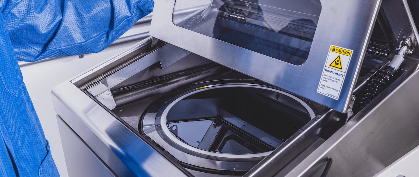
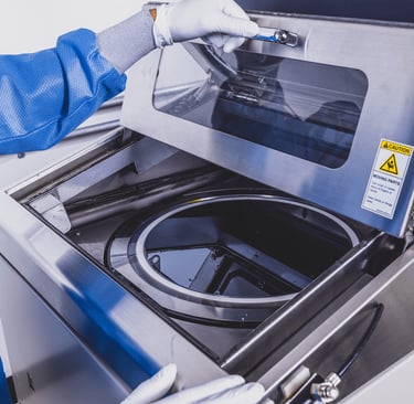
Backgrinding for 8” and 12” Wafers
Modern semiconductor manufacturing (logic, memory, CIS) overwhelmingly uses grinding instead of lapping.
Why backgrinding is ideal for larger wafers
Large wafers are flexible and require single-side controlled removal
Tape protection on the device side prevents contamination
Better control over:
Total thickness variation (TTV)
Subsurface micro-damage
Stress distribution
Compatible with temporary bonding systems for ultra-thin (<50 µm) targets
Process flow
Front-side tape mounting
Protects circuitry and stabilizes the wafer.Coarse grinding
High-removal diamond wheels eliminate most bulk silicon.Fine grinding
Uses ultra-fine grit wheels (<3000 grit) for smooth surface finish.Stress-relief etching or CMP (optional)
Removes micro-cracks and reduces warpage.Debonding / tape removal
For extremely thin wafers, UV-release or laser-release tapes are preferred.
Final Thoughts
Wafer backgrinding sits at the intersection of materials science, mechanical engineering, and precision manufacturing. The choice of thinning method—lapping for small, rigid wafers or advanced grinding for modern large-diameter silicon—depends heavily on wafer size, mechanical strength, and desired final thickness.
As devices continue pushing toward thinner profiles and more advanced packaging architectures, the integration of fine grinding, stress-relief processes, and temporary bonding will remain a key enabler for next-generation semiconductor performance.