
Leaded vs Lead-Free Solder Bumps
A detailed comparison of leaded and lead-free solder bumps, explaining material differences, process impacts, and reliability trade-offs in modern semiconductor wafer bumping and flip-chip packaging.
1/6/20266 min read
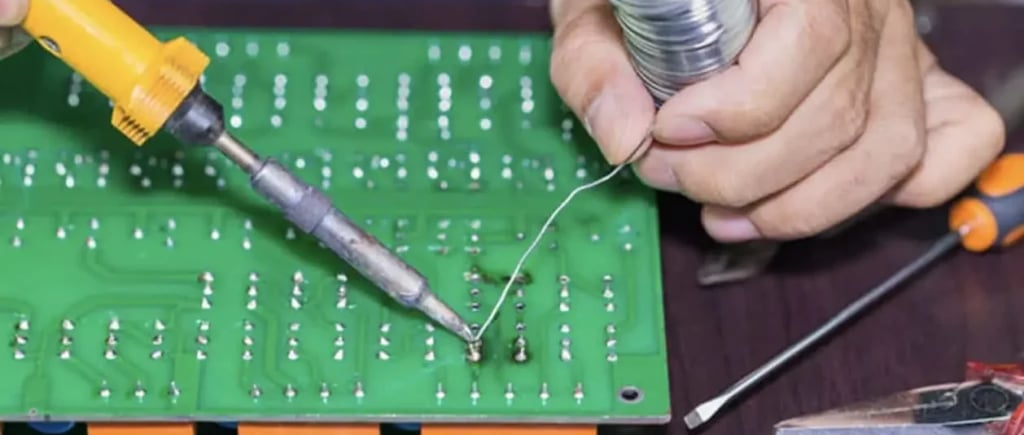
This image shows lead-free solder being applied during electronic assembly, illustrating modern solder materials used in compliant semiconductor and PCB interconnect processes.
Leaded vs Lead-Free Solder Bumps: Materials, Reliability, and Manufacturing Trade-Offs
Solder bump technology is a cornerstone of modern wafer bumping and flip-chip packaging. These microscopic interconnects provide both electrical connectivity and mechanical attachment between semiconductor dies and substrates. While bump geometry and under-bump metallization are critical, the solder alloy itself plays a decisive role in manufacturability, reliability, and long-term performance.
For decades, leaded solder bumps dominated semiconductor packaging due to their forgiving process behavior and proven reliability. However, regulatory pressure, environmental considerations, and evolving industry standards have driven a widespread transition to lead-free solder bumps. This shift is not simply a material substitution; it fundamentally alters process windows, failure mechanisms, and reliability behavior.
Understanding the differences between leaded and lead-free solder bumps is essential for backend engineers, packaging designers, and reliability teams. This article provides a detailed comparison of the two, focusing on material properties, process integration, reliability trade-offs, and application-driven selection criteria.
The Role of Solder Bumps in Semiconductor Packaging
Solder bumps serve as the physical and electrical interface between a semiconductor die and its package or substrate. During flip-chip assembly, solder bumps are reflowed to create metallurgical bonds with substrate pads, enabling direct signal routing and efficient heat dissipation.
Beyond electrical conduction, solder bumps absorb mechanical stress caused by thermal expansion mismatch between silicon and organic or ceramic substrates. Their ability to deform plastically under stress is a key factor in long-term reliability.
Because solder bumps operate at the intersection of electrical, thermal, and mechanical domains, the choice of solder alloy has far-reaching consequences.
What Are Leaded Solder Bumps?
Leaded solder bumps typically use high-lead alloys, most commonly tin-lead (SnPb) compositions with lead content ranging from 85% to 97%. These alloys have been used extensively in flip-chip and ceramic package applications for decades.
High-lead solder bumps are characterized by:
Relatively low modulus and high ductility
Stable, predictable intermetallic behavior
Wide process windows during reflow
Leaded solder bumps were historically favored in high-reliability applications such as aerospace, defense, and early automotive electronics due to their fatigue resistance and long field history.
What Are Lead-Free Solder Bumps?
Lead-free solder bumps replace lead with alternative alloying elements, most commonly silver and copper. The most widely used lead-free alloys are SAC (tin-silver-copper) systems, such as SAC305 (96.5Sn-3Ag-0.5Cu).
Lead-free solder bumps were introduced primarily to comply with environmental regulations such as RoHS. Over time, they have become the industry standard for most consumer, automotive, and industrial semiconductor products.
Lead-free solder bumps exhibit:
Higher melting temperatures
Increased stiffness compared to leaded alloys
Different intermetallic growth behavior
These differences significantly impact both processing and reliability.
Regulatory and Environmental Drivers
The transition from leaded to lead-free solder bumps was largely driven by environmental and health regulations. Lead is a toxic material, and its use in electronics has been restricted in many regions.
Regulatory compliance requirements have made lead-free solder mandatory for most commercial electronics. However, exemptions still exist for certain high-reliability and specialty applications where leaded solder remains acceptable.
As a result, many manufacturers now operate dual solder bump ecosystems, supporting both leaded and lead-free technologies depending on customer and application requirements.
Material Property Differences
Melting Temperature
Leaded solder bumps typically melt at lower temperatures than lead-free alternatives. High-lead alloys have melting points around 300 °C, while eutectic SnPb melts at 183 °C. Lead-free SAC alloys melt around 217–220 °C.
Higher melting temperatures increase thermal stress on dies, under-bump metallization, and substrates during reflow. This narrows the process window and increases the importance of temperature control.
Mechanical Behavior
Leaded solder alloys are generally more ductile and better at absorbing cyclic strain. This makes them more forgiving under thermal cycling and mechanical shock.
Lead-free alloys are stiffer and exhibit higher elastic modulus. While this improves mechanical strength, it can also increase stress transfer to interfaces, accelerating fatigue or cracking in some conditions.
Process Integration and Manufacturing Impact
Reflow Profiles
Leaded solder bumps allow broader reflow profiles with lower peak temperatures. Lead-free solder bumps require tighter thermal control and higher peak temperatures, increasing the risk of:
Die warpage
UBM degradation
Substrate damage
Optimizing reflow profiles is more critical in lead-free processes, especially for thin dies and fine-pitch designs.
Wetting and Self-Alignment
Leaded solder bumps typically exhibit excellent wetting and self-alignment behavior during reflow. This helps compensate for minor placement errors during assembly.
Lead-free solders generally have poorer wetting characteristics, requiring more precise placement accuracy and well-designed under-bump metallization to ensure uniform bump collapse.
Intermetallic Compound Formation
Intermetallic compound (IMC) formation is inevitable in solder bump systems and plays a major role in reliability.
Leaded solder bumps tend to form relatively stable and predictable IMC layers with nickel-based UBMs. Growth rates are slower, and IMCs tend to be less brittle.
Lead-free solder bumps form different IMC phases that can grow more rapidly, especially at elevated temperatures. Excessive IMC growth can lead to brittle interfaces and increased susceptibility to cracking under thermal cycling.
Managing IMC behavior is one of the biggest challenges in lead-free solder bump design.
Reliability Under Thermal Cycling
Thermal cycling is one of the most important reliability tests for solder bumps. Repeated expansion and contraction place cyclic strain on the bump and its interfaces.
Leaded solder bumps generally outperform lead-free bumps in long-term thermal cycling due to their higher ductility and strain-relief capability.
Lead-free solder bumps can still meet automotive and industrial reliability requirements, but often require:
Optimized bump geometry
Improved UBM design
Careful substrate material selection
Reliability margins tend to be narrower in lead-free systems.
Electrical and Power Performance
From an electrical standpoint, both leaded and lead-free solder bumps provide adequate conductivity for most applications. Differences in resistivity are usually negligible at the bump scale.
However, lead-free solder bumps often operate at higher temperatures due to higher reflow and operating limits. This can accelerate electromigration and thermal aging in high-current applications if not properly managed.
Power devices and high-current interconnects often require additional design margins when using lead-free solder.
Fine-Pitch and Advanced Packaging Considerations
As bump pitch decreases, material differences become more pronounced.
Leaded solder bumps are easier to process at larger pitches but struggle to scale to very fine pitches due to collapse control and bridging risks.
Lead-free solder bumps, especially when combined with copper pillar structures, offer better scalability to fine-pitch applications. Copper pillars reduce solder volume and improve dimensional control, mitigating some limitations of lead-free alloys.
As a result, most advanced logic and mobile devices use lead-free solder in combination with copper pillars rather than traditional solder spheres.
Automotive and High-Reliability Applications
Automotive electronics impose strict reliability requirements, including wide temperature ranges and long service lifetimes.
Early automotive designs favored leaded solder bumps for their fatigue resistance. Today, most automotive applications have transitioned to lead-free solder bumps, driven by regulatory alignment and improved material understanding.
However, automotive lead-free implementations typically involve:
Conservative design margins
Extensive reliability testing
Robust UBM and substrate design
Leaded solder may still be used in niche, exempted applications where maximum fatigue resistance is required.
Cost and Supply Chain Considerations
Leaded solder alloys are generally simpler to process and may offer lower manufacturing risk in certain legacy systems. However, regulatory compliance and shrinking supplier ecosystems can increase long-term risk.
Lead-free solder bumps align with global supply chains and regulatory requirements but often involve higher process complexity and tighter control.
Cost decisions must consider not only material price, but also yield impact, reliability risk, and long-term availability.
Choosing Between Leaded and Lead-Free Solder Bumps
There is no universally “better” option. The correct choice depends on application requirements, regulatory constraints, and manufacturing capability.
Leaded solder bumps may be preferred when:
Maximum thermal fatigue resistance is required
Regulatory exemptions apply
Legacy processes must be maintained
Lead-free solder bumps are preferred when:
Regulatory compliance is mandatory
Fine-pitch scalability is required
Integration with modern packaging platforms is needed
In many organizations, both technologies coexist.
Backend Manufacturing Support with Silicon Craft Technologies
Selecting and implementing the right solder bump technology requires deep understanding of materials, process integration, and reliability behavior. Silicon Craft Technologies provides backend manufacturing support to help customers evaluate leaded and lead-free solder bump options within their specific packaging and reliability requirements.
With experience in wafer bumping, UBM design, assembly process optimization, and reliability qualification, Silicon Craft Technologies works closely with customers to balance manufacturability, compliance, and long-term performance. Their collaborative approach supports low-to-medium volume production, advanced packaging development, and smooth technology transitions.
Conclusion
The transition from leaded to lead-free solder bumps represents one of the most significant material shifts in semiconductor packaging. While lead-free technologies now dominate the industry, leaded solder bumps continue to play a role in specific high-reliability and exempted applications.
Understanding the material, process, and reliability differences between leaded and lead-free solder bumps enables informed decision-making and robust package design. With proper optimization, both technologies can deliver reliable performance—but only when their limitations are fully understood and addressed.