
Modern Wafer Dicing Techniques: A Deep Dive
Explore how modern wafer dicing technologies are transforming semiconductor manufacturing. This in-depth Si-Craft article compares blade, laser, plasma, and stealth dicing methods — detailing their processes, advantages, and challenges — to help engineers choose the right technique for today’s ultra-thin, high-precision wafers.
10/2/20254 min read
Introduction
In semiconductor manufacturing, the wafer dicing process — the precise separation of a processed wafer into individual dies — is one of the most critical steps in ensuring product yield, device integrity, and overall cost efficiency.
Every integrated circuit begins life as part of a larger wafer, and how that wafer is divided can determine whether thousands of chips function perfectly or fail due to stress and contamination. As device geometries shrink and wafers become thinner, traditional cutting techniques face new challenges.
Modern innovations such as laser, plasma, and stealth dicing are transforming how manufacturers like Si-Craft approach die singulation — reducing mechanical stress, minimizing debris, and improving yield on advanced materials and ultra-thin wafers.
Understanding Wafer Dicing
A semiconductor wafer is a thin, circular substrate of material — most commonly silicon — that contains hundreds or thousands of identical integrated circuits. Once fabrication is complete, these circuits must be separated cleanly and efficiently for packaging and assembly.
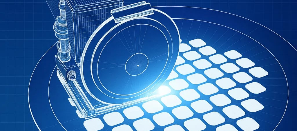
Wafer dicing, also known as die singulation, performs this separation. The goal is to cut through the wafer streets (the narrow spaces between dies) with minimal chipping, cracking, or contamination, while maintaining the structural integrity of each die.
Primary Wafer Dicing Techniques
1. Blade Dicing (Mechanical Saw)
Process
A high-speed, diamond-coated blade rotates along the wafer streets to physically cut through the material. The wafer is mounted on an adhesive film stretched across a support frame to hold the individual dies in place during cutting.
Advantages
Mature, reliable, and widely used in high-volume manufacturing
Fast throughput and low cost per wafer
Straightforward process integration with standard equipment
Limitations
Introduces mechanical stress, leading to chipping or micro-cracks
Generates debris that requires post-cleaning
Relatively wide kerf width reduces the number of dies per wafer
Typical Use
Ideal for standard silicon wafers, moderate die sizes, and cost-sensitive, high-volume production where slight edge damage is acceptable.
2. Laser Dicing
Process
A tightly focused laser beam ablates or modifies the wafer material along predefined cut lines. Depending on the application, the laser can operate in ultraviolet, infrared, or visible ranges, often using pulsed or ultra-short pulses to minimize thermal effects.
Advantages
Non-contact process with minimal mechanical stress
Enables narrower kerf widths and closer die spacing
Suitable for thin and brittle wafers where mechanical dicing would cause damage
Limitations
Equipment cost is higher and process setup more complex
Thermal effects can cause localized damage if not well controlled
Slightly slower throughput compared to mechanical saws
Typical Use
Preferred for thin wafers, fragile materials, or high-density layouts where die integrity and precision outweigh throughput and cost considerations.
3. Plasma Dicing (Dry Etch Separation)
Process
Plasma dicing uses a reactive ion etching process to remove material along the wafer streets. It is a non-mechanical, chemical-based approach that completely eliminates physical contact with the wafer surface.
Advantages
Zero mechanical stress, preventing cracks and chipping
Extremely narrow cut lines allow higher die counts per wafer
Produces clean, debris-free surfaces ideal for sensitive devices
Limitations
Requires specialized plasma equipment and longer processing times
Higher initial cost and process complexity
Not yet standardized for all wafer materials
Typical Use
Best for ultra-thin or brittle wafers, high-reliability applications, and advanced packaging technologies where die edge quality and cleanliness are paramount.
4. Stealth Dicing
Process
Stealth dicing uses a focused laser beam to create internal modification planes inside the wafer without cutting through the surface. The wafer is later separated (cleaved) along these modified regions.
Advantages
Extremely high precision and minimal surface damage
Virtually no debris or contamination
Excellent for ultra-thin wafers and MEMS devices
Limitations
Higher equipment and operational costs
Slightly lower throughput than mechanical dicing
Requires advanced process control for consistent results
Typical Use
Ideal for ultra-thin, high-reliability applications such as MEMS, optical components, and advanced semiconductor packages.
Key Challenges
Even with process improvements, wafer dicing presents consistent engineering and production challenges:
Die Chipping and Cracking — Excessive stress from cutting can create micro-cracks that compromise yield and long-term reliability.
Contamination and Debris — Blade and laser dicing produce debris that must be removed to prevent packaging contamination.
Precision Limitations — Shrinking die sizes and tighter spacing push mechanical dicing beyond its physical limits.
Material Diversity — New materials such as GaN, SiC, and glass require methods that minimize stress and heat.
Process Integration — Dicing quality directly affects downstream bonding, encapsulation, and final testing.
Innovations and Future Directions
Modern dicing methods are evolving rapidly. Key areas of advancement include:
Ultrashort-Pulse Lasers — Deliver cleaner cuts with minimal heat-affected zones.
Multi-Beam and Parallel Processing — Improves throughput for laser systems.
Plasma Dicing for Narrow Streets — Allows smaller dies and higher wafer utilization.
Self-Dicing Materials — Engineered wafers that naturally cleave along designed lines.
Automated Inspection and Data-Driven Control — Real-time monitoring and defect detection improve process reliability.
These innovations align with the semiconductor industry’s shift toward thinner wafers, higher density, and increasingly complex packaging.
Si-Craft’s Perspective
At Si-Craft Technologies, we view wafer dicing as a strategic enabler of performance and yield. Choosing the right method depends on the balance between material type, die geometry, cost, and reliability.
Our approach emphasizes:
Evaluating material brittleness and wafer thickness before process selection
Implementing inline inspection and statistical process control for dicing quality
Piloting laser and plasma methods for upcoming ultra-thin and advanced device nodes
Continuously benchmarking yield versus cost to determine the optimal production mix
By combining traditional expertise with cutting-edge innovation, Si-Craft ensures that each die we produce meets the highest standards of precision, cleanliness, and reliability.
Conclusion
Wafer dicing is no longer just a mechanical cutting process — it is a precision operation that defines the quality, yield, and scalability of modern semiconductors.
Mechanical blade dicing continues to dominate cost-driven production, but advanced methods such as laser, plasma, and stealth dicing are increasingly essential for thin wafers, brittle materials, and next-generation devices.
As the industry pushes toward miniaturization and integration, mastering these techniques will enable manufacturers to produce cleaner cuts, reduce waste, and achieve higher reliability — setting the stage for the next era of semiconductor innovation.