
Pad Metallurgy Impact on Bond Quality
A detailed guide on how pad metallurgy influences wire bond quality, covering material choices, pad stack design, common failure modes, and reliability considerations in semiconductor backend manufacturing.
Kiran
1/6/20265 min read
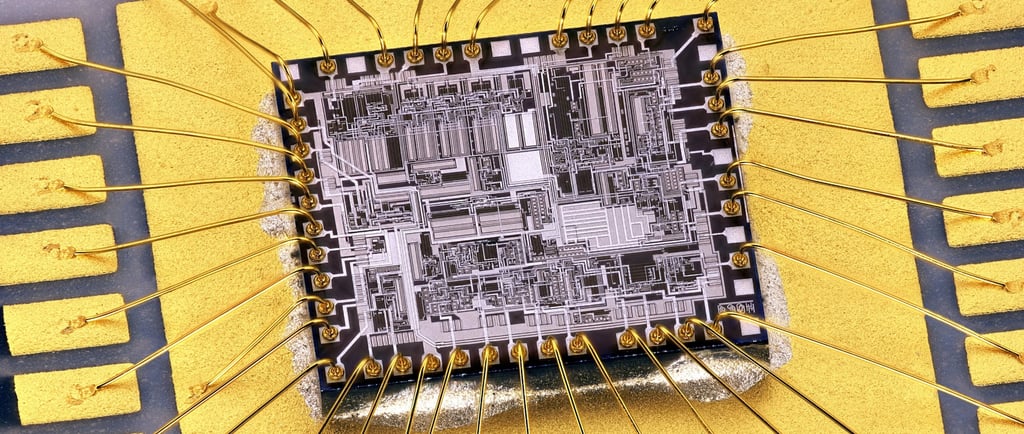
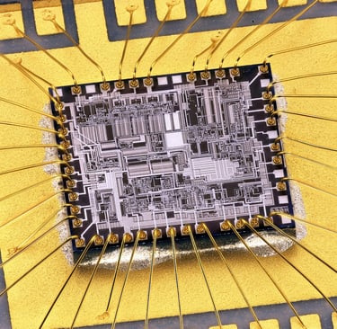
This image shows gold wire bonds formed on a semiconductor die, highlighting the role of pad metallurgy in bond formation, interconnect reliability, and overall wire bond quality.
Pad Metallurgy Impact on Bond Quality: Why the Bond Pad Matters More Than You Think
In wire bonding, attention often focuses on wire material, ultrasonic energy, bond force, and loop geometry. While these parameters are critical, one factor consistently determines whether a bond succeeds or fails: pad metallurgy. The bond pad is the interface where electrical, mechanical, and metallurgical interactions converge. If the pad metallurgy is poorly designed, incompatible, or poorly controlled, even a well-optimized wire bonding process can produce weak, unreliable, or latent defects.
As semiconductor devices move toward finer pitches, thinner die stacks, and more complex backend integration, pad metallurgy has become one of the most important—and most overlooked—contributors to bond quality. This article examines how pad metallurgy influences bond formation, common pad-related failure modes, and best practices for designing and controlling pad stacks to ensure robust wire bonding performance.
What Is Pad Metallurgy?
Pad metallurgy refers to the composition, thickness, and layer structure of the metal stack used to form the wire bond pad on the semiconductor die. The pad must serve several functions simultaneously:
Provide a clean, bondable surface
Maintain electrical conductivity
Protect underlying dielectric layers
Withstand mechanical and thermal stress during bonding and operation
A typical pad is not a single metal layer but a multilayer stack engineered to balance adhesion, conductivity, and mechanical robustness.
Common Pad Metallurgy Systems
Aluminum-Based Pad Metallurgy
Aluminum and aluminum alloys remain the most widely used pad materials in wire-bonded devices.
Common variants include:
Pure aluminum (Al)
Aluminum-copper alloys (AlCu)
Aluminum-silicon alloys (AlSi)
Aluminum pads are compatible with both gold and aluminum wire bonding and offer good electrical performance. However, aluminum readily forms a native oxide layer that must be disrupted during bonding.
Gold-Based Pad Metallurgy
Gold pads are often used in specialty devices, RF applications, or where corrosion resistance is critical. Gold provides an oxide-free surface, simplifying bond formation.
However, gold pads introduce challenges such as:
Intermetallic growth with gold wire
Cost considerations
Compatibility issues with copper wire
Copper-Based Pad Metallurgy
Copper pad metallization is increasingly used in advanced nodes due to copper’s superior conductivity. Copper pads typically require barrier and cap layers to prevent oxidation and diffusion.
Copper pads present significant wire bonding challenges due to:
Rapid oxide formation
Higher hardness compared to aluminum
Narrower bonding process windows
Pad Stack Structure and Its Role in Bond Quality
The pad stack extends beyond the top metal layer. Beneath the bondable surface are adhesion layers, diffusion barriers, and dielectric materials.
Top Metal Thickness
Pad thickness directly affects bond robustness. Thin pads:
Are more susceptible to cratering
Offer limited energy absorption
Increase risk of pad lift or cracking
As devices scale down, pad thickness often decreases, making process control more critical.
Barrier and Adhesion Layers
Barrier layers (e.g., Ti, TiN, TaN) prevent diffusion between metals and underlying layers. Poor barrier integrity can lead to:
Delamination
Electrical leakage
Long-term reliability failures
Dielectric Support
Low-k and ultra-low-k dielectrics reduce capacitance but provide less mechanical support. Pads built on weak dielectrics are more prone to:
Cratering during bonding
Subsurface cracking
Latent reliability issues
How Pad Metallurgy Influences Bond Formation
Oxide Disruption
Bond formation requires intimate metal-to-metal contact. Oxide layers on aluminum or copper pads must be disrupted through:
Ultrasonic energy
Bond force
Localized friction
Pads with thick or tenacious oxide layers require higher energy, increasing the risk of pad damage.
Intermetallic Formation
Intermetallic compounds (IMCs) form at the bond interface and contribute to bond strength. The type, growth rate, and morphology of IMCs depend strongly on pad metallurgy.
Poorly controlled IMC growth can lead to:
Brittle interfaces
Kirkendall voiding
Long-term bond degradation
Pad Metallurgy and Wire Material Compatibility
Aluminum Pad with Gold Wire
This is one of the most common combinations, but it carries the risk of purple plague (AuAl₂ intermetallic formation) at elevated temperatures.
Mitigation strategies include:
Controlled bonding temperatures
Optimized ultrasonic energy
Barrier layer engineering
Aluminum Pad with Aluminum Wire
Aluminum-to-aluminum bonding offers excellent compatibility and avoids dissimilar metal IMCs. However, it typically requires higher ultrasonic energy to break oxide layers.
Copper Pad with Gold or Copper Wire
Copper pads are more challenging due to oxidation and hardness. Successful bonding requires:
Aggressive surface preparation
Narrow process windows
Enhanced barrier and cap layer design
Common Pad-Related Failure Modes
Pad Lift
Pad lift occurs when the bond pad separates from the underlying layers. Causes include:
Poor adhesion layer design
Excessive bonding force
Weak dielectric support
Pad lift is often catastrophic and difficult to detect visually.
Cratering
Cratering is subsurface damage beneath the bond pad, typically in the dielectric layer. It is strongly associated with:
Thin pad stacks
Low-k dielectrics
Excessive ultrasonic energy
Cratering may not cause immediate failure but can lead to latent reliability issues.
Interfacial Delamination
Delamination between pad layers can occur due to:
Thermal cycling
Moisture ingress
Poor barrier integrity
This failure mode often appears after environmental stress testing.
Impact of Fine-Pitch Scaling on Pad Metallurgy
As pad pitch decreases:
Pad area shrinks
Pad thickness often reduces
Mechanical margins narrow
These trends amplify the impact of pad metallurgy on bond quality. Fine-pitch wire bonding places higher stress per unit area on the pad, making pad stack design a limiting factor rather than the bonding process itself.
Advanced devices increasingly require co-optimization of pad design and bonding parameters rather than independent optimization.
Inspection and Testing for Pad Metallurgy Issues
Detecting pad-related issues requires more than standard optical inspection.
Common methods include:
Wire pull and shear testing with failure mode analysis
Cross-sectioning and metallography
Scanning acoustic microscopy
Electrical stress testing
Failure mode trends often provide the earliest indication of pad metallurgy problems.
Pad Metallurgy in Reliability Qualification
Reliability testing frequently exposes weaknesses in pad metallurgy that are not apparent during initial testing.
Stress conditions such as:
Thermal cycling
High-temperature storage
Humidity testing
can accelerate interfacial degradation, revealing pad adhesion or dielectric support issues. Devices that pass initial pull and shear tests may still fail after prolonged stress if pad metallurgy is marginal.
Best Practices for Optimizing Pad Metallurgy
Key best practices include:
Designing pad stacks with sufficient thickness and support
Selecting wire materials compatible with pad metallurgy
Minimizing oxide formation through process control
Co-optimizing bonding parameters with pad design
Validating through aggressive reliability testing
Pad metallurgy should be treated as a critical design parameter, not a fixed constraint.
Backend Manufacturing Support with Silicon Craft Technologies
Managing pad metallurgy challenges requires close coordination between design, wafer fabrication, and backend assembly. Silicon Craft Technologies provides engineering-driven backend manufacturing support to address these complex interactions.
With experience in wire bonding process development, pad-related failure analysis, and reliability qualification, Silicon Craft Technologies helps customers evaluate pad stack robustness, optimize bonding parameters, and mitigate latent risks. Their collaborative approach supports low-to-medium volume production, advanced package development, and smooth transition from design to manufacturing.
By integrating pad metallurgy considerations into backend process strategy, Silicon Craft Technologies enables stronger bonds, higher yield, and improved long-term reliability.
Conclusion
Pad metallurgy plays a decisive role in wire bond quality, reliability, and yield. As device geometries shrink and backend processes become more demanding, the pad is no longer a passive element—it is an active contributor to success or failure.
Understanding how pad composition, thickness, and underlying support interact with bonding energy and wire material is essential for modern semiconductor packaging. When pad metallurgy is properly designed and controlled, wire bonding remains a robust and reliable interconnect technology even at advanced nodes.