
RDL Thickness Optimization
A practical guide to RDL thickness optimization, explaining how redistribution layer thickness impacts electrical performance, reliability, manufacturability, and cost in advanced semiconductor packaging.
Kiran
1/6/20265 min read
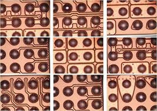
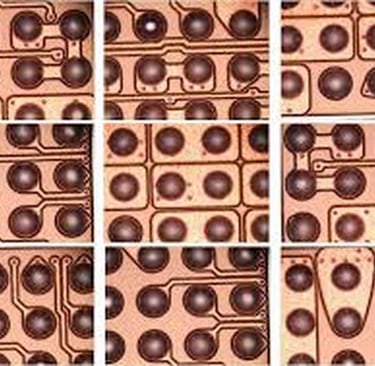
This image shows copper redistribution layer patterns used to evaluate RDL thickness uniformity, a critical factor in electrical performance, reliability, and yield in advanced semiconductor packaging.
RDL Thickness Optimization: Balancing Electrical Performance, Reliability, and Manufacturability
Redistribution layers (RDLs) have become a foundational element of modern semiconductor packaging. As packaging technologies evolve toward fan-out wafer-level packaging, advanced wafer-level packages, and heterogeneous integration, RDLs enable signal rerouting, pitch conversion, and multi-die interconnects that are no longer possible with traditional substrates alone. While RDL layout and material selection receive significant attention, RDL thickness optimization is equally critical and often underestimated.
RDL thickness directly influences electrical resistance, current carrying capability, mechanical stress, yield stability, and long-term reliability. A thickness that is too thin can cause excessive voltage drop, electromigration, or cracking. A thickness that is too thick can introduce stress, warpage, lithography challenges, and unnecessary cost. Optimizing RDL thickness is therefore a balancing act that must consider electrical, mechanical, thermal, and manufacturing constraints simultaneously.
This article provides a comprehensive explanation of RDL thickness optimization, examining why thickness matters, how it is selected, what trade-offs are involved, and how manufacturers validate thickness decisions for reliable high-volume production.
The Role of RDL in Advanced Packaging
Redistribution layers are thin-film metal interconnects formed on wafers or reconstituted wafers to reroute signals from die pads to new locations. They enable area-array interconnects, larger pitch solder bumps, and integration of multiple dies into a single package.
RDLs must carry electrical signals and power while also surviving thermal cycling, mechanical stress, and downstream assembly processes. Because RDLs are fabricated using thin-film processes rather than bulk copper traces, their thickness becomes a dominant design variable.
Unlike traditional substrates where copper thicknesses are measured in tens of microns, RDL thicknesses typically range from a few microns to low double-digit microns. Within this range, even small changes in thickness can significantly affect performance and reliability.
Why RDL Thickness Matters
RDL thickness determines the cross-sectional area of the conductor, which directly impacts electrical resistance. Thinner RDLs have higher resistance, leading to voltage drop, signal degradation, and localized heating, particularly in power and ground lines.
Thickness also affects mechanical behavior. Thin RDLs are more flexible but may be prone to cracking or electromigration. Thick RDLs provide mechanical robustness but can introduce stress concentration, dielectric cracking, or wafer warpage.
From a manufacturing perspective, RDL thickness influences lithography resolution, plating time, planarization requirements, and defect sensitivity. Optimization must therefore align electrical design goals with realistic manufacturing capability.
Electrical Performance and Thickness Trade-Offs
One of the primary drivers of RDL thickness selection is electrical performance. Resistance decreases as thickness increases, improving signal integrity and reducing power loss.
For high-speed signals, RDL thickness interacts with line width and dielectric properties to determine impedance. While thickness alone does not define impedance, it affects conductor loss and current distribution.
For power delivery networks, insufficient RDL thickness can cause localized heating and accelerated electromigration, especially in fan-out packages where power routing relies heavily on thin-film metals.
However, increasing thickness beyond what is electrically required offers diminishing returns. Excess thickness increases cost, stress, and processing complexity without proportional electrical benefit.
Current Carrying Capacity and Electromigration
Electromigration is a major reliability concern in RDL structures, particularly as current density increases. Thin RDLs concentrate current in a small cross-sectional area, accelerating atomic migration and void formation.
Optimizing thickness reduces current density and improves electromigration lifetime. This is especially critical for:
Power and ground lines
High-duty-cycle signals
Automotive and industrial applications
However, electromigration resistance is also influenced by grain structure, copper purity, and barrier layers. Thickness optimization must be paired with material and process control to achieve reliable results.
Mechanical Stress and Warpage Considerations
RDL thickness contributes to the overall stress profile of the package. Thick copper layers have a higher coefficient of thermal expansion mismatch with surrounding dielectrics, increasing stress during thermal cycling.
In fan-out wafer-level packaging, RDL thickness directly affects wafer warpage. Excessive warpage can cause lithography misalignment, plating non-uniformity, and assembly defects.
Thin RDLs reduce warpage but may lack mechanical robustness. Optimized designs often use variable thickness, with thicker power traces and thinner signal lines, to balance stress and performance.
Dielectric Interaction and RDL Stack Design
RDL thickness cannot be optimized in isolation. It must be considered alongside dielectric thickness, material properties, and stack symmetry.
Thick RDLs on thin dielectrics can induce cracking or delamination. Conversely, thick dielectrics with thin RDLs may suffer from poor heat dissipation and higher resistance.
Balanced RDL stacks distribute stress more evenly and improve reliability. This is particularly important in multi-layer RDL structures, where cumulative stress can become significant.
Lithography and Patterning Constraints
As RDL thickness increases, lithography becomes more challenging. Thick photoresist layers are required to define thick copper traces, increasing the risk of pattern collapse, poor resolution, and incomplete development.
Fine-pitch RDL designs place additional limits on thickness. Narrow lines cannot support excessive thickness without risking overplating, sidewall roughness, or bridging.
RDL thickness optimization must therefore account for achievable line width, spacing, and process margin in high-volume manufacturing.
Plating Uniformity and Process Control
Electroplating is the most common method for forming RDL copper. Plating uniformity across the wafer or panel becomes more difficult as thickness increases.
Non-uniform thickness leads to:
Resistance variation
Localized stress concentration
Assembly yield loss
Optimized thickness targets are chosen to maintain acceptable uniformity without excessive plating time or chemistry complexity.
Single-Layer vs Multi-Layer RDL Thickness Strategy
In simple fan-out designs, a single RDL layer may be sufficient. In more complex packages, multiple RDL layers are stacked to route signals and power.
Thickness optimization strategies differ between these cases. Single-layer RDLs may require greater thickness to carry power, while multi-layer stacks can distribute current across layers.
Multi-layer RDL designs often use thinner individual layers to reduce stress while achieving overall routing density.
Reliability Testing and Validation
RDL thickness decisions must be validated through reliability testing. Common tests include:
Thermal cycling
Temperature-humidity bias
Power cycling
Mechanical bending or drop testing
Failures such as cracking, delamination, or resistance increase often indicate that RDL thickness is not well matched to material properties and package geometry.
Successful designs demonstrate stable electrical performance and mechanical integrity throughout qualification testing.
Cost and Throughput Considerations
Thicker RDLs increase plating time, material consumption, and inspection complexity. This directly affects cost and cycle time.
Optimized thickness targets aim to meet performance and reliability requirements with minimal excess. Overdesigning thickness may provide marginal reliability benefit at disproportionate cost.
Cost-aware optimization is particularly important in high-volume consumer and automotive markets.
Application-Specific Thickness Optimization
RDL thickness requirements vary significantly by application.
High-performance computing and networking devices prioritize low resistance and power integrity, often requiring thicker RDLs.
Mobile and wearable devices prioritize thin form factors and low warpage, favoring thinner RDLs with careful routing.
Automotive and industrial applications emphasize long-term reliability, often leading to conservative thickness choices validated through extensive testing.
There is no universal thickness value; optimization must be application-driven.
Common Failure Modes Linked to Poor Thickness Optimization
Improper RDL thickness selection can lead to:
Electromigration-induced opens
Cracking due to thermal stress
Delamination at dielectric interfaces
Excessive warpage affecting assembly
Many of these failures appear only after stress testing or field use, making early optimization essential.
Backend Manufacturing Support with Silicon Craft Technologies
Optimizing RDL thickness requires close coordination between design intent, material selection, process capability, and reliability validation. Silicon Craft Technologies provides backend manufacturing support to help customers define and qualify RDL thickness strategies for advanced packaging.
With experience across fan-out wafer-level packaging, multi-layer RDL integration, and reliability qualification, Silicon Craft Technologies works with customers to balance electrical performance, manufacturability, and long-term stability. Their collaborative approach supports early design decisions as well as production ramp and yield improvement.
Conclusion
RDL thickness optimization is a critical design and manufacturing decision that directly affects electrical performance, mechanical reliability, yield, and cost. Too thin, and reliability suffers. Too thick, and manufacturability and stress become limiting factors.
Successful RDL designs strike a careful balance, guided by application requirements, material behavior, and process capability. As advanced packaging continues to evolve, thoughtful RDL thickness optimization will remain essential to delivering reliable, high-performance semiconductor products.