
Silicon vs Compound Semiconductor Wafers: Processing Differences Explained
Explore the key processing differences between silicon and compound semiconductor wafers—and how they impact performance, yield, and manufacturing complexity.
Kiran
1/5/20266 min read
Silicon vs Compound Semiconductor Wafers: Processing Differences Explained
The semiconductor industry has long relied on silicon as its foundational material, enabling decades of scaling, cost reduction, and manufacturing standardization. However, as system requirements increasingly emphasize power efficiency, high-frequency operation, wide bandgap performance, and optical functionality, compound semiconductors have become indispensable. Materials such as gallium arsenide (GaAs), silicon carbide (SiC), and gallium nitride (GaN) now underpin critical technologies in power electronics, RF communication, and optoelectronics.
Although silicon and compound semiconductor wafers share similar outward form factors, their processing requirements differ fundamentally. These differences are not cosmetic or incremental; they are rooted in intrinsic material properties that influence crystal growth, wafer preparation, device fabrication, backend processing, and yield behavior. Understanding these distinctions is essential for engineers, process developers, and manufacturing teams working across heterogeneous technology platforms.
This article examines the key processing differences between silicon and compound semiconductor wafers, with an emphasis on how material physics translates into practical manufacturing constraints and trade-offs.
Material Fundamentals Driving Process Divergence
At the most basic level, silicon is a single-element semiconductor with a well-understood crystal structure, mechanical behavior, and thermal response. Its covalent bonding and relatively low lattice defect density make it highly tolerant to aggressive processing conditions. Over time, the industry has refined silicon processing to an extraordinary degree, enabling consistent results across large wafers and high-volume production.
Compound semiconductors, by contrast, consist of two or more elements combined in a specific stoichiometric ratio. These materials offer superior electronic or optical properties for targeted applications, but that performance comes at the cost of increased processing sensitivity. Differences in atomic mass, bonding energy, and lattice structure introduce challenges in crystal growth, defect control, and thermal stability that directly affect manufacturability.
The result is not simply a different process recipe, but an entirely different manufacturing philosophy—one that prioritizes control, selectivity, and compromise over brute-force scalability.
Crystal Growth and Wafer Formation
Silicon Crystal Growth and Scalability
Silicon wafers are primarily grown using the Czochralski or float-zone methods, both of which are highly mature and tightly controlled. These processes enable the production of large-diameter single crystals with low defect densities and uniform electrical properties. Today, 300 mm silicon wafers are the industry standard for advanced logic and memory, with well-established infrastructure supporting high-volume manufacturing.
The maturity of silicon crystal growth underpins its economic advantage. High yields, reproducible quality, and large wafer area allow fixed processing costs to be amortized across millions of devices.
Compound Semiconductor Crystal Growth Complexity
Compound semiconductor crystal growth is inherently more complex. Techniques such as vertical gradient freeze, hydride vapor phase epitaxy, metal-organic chemical vapor deposition, and ammonothermal growth are used depending on the material system. Each method must carefully balance composition, temperature gradients, and growth rates to maintain stoichiometry.
Defects such as dislocations, micropipes, and stacking faults are more prevalent, and wafer diameters are correspondingly smaller. While progress has been made toward 200 mm substrates for some materials, most compound semiconductor manufacturing still relies on 100 mm or 150 mm wafers, limiting throughput and increasing cost per unit area.
Mechanical Properties and Wafer Handling
Mechanical Robustness of Silicon
Silicon wafers exhibit relatively high fracture toughness and predictable mechanical behavior. This robustness allows them to withstand automated handling, high-speed transport, and aggressive thinning during backend processing. With appropriate support, silicon wafers can be thinned to well below 100 microns while remaining compatible with automated assembly flows.
This mechanical resilience is a key enabler of high-volume manufacturing and complex backend integration.
Brittleness and Fragility of Compound Semiconductors
Most compound semiconductor wafers are significantly more brittle than silicon. Materials such as GaAs and InP are prone to edge chipping and crack propagation, while SiC—despite its hardness—can fail catastrophically due to internal defects. This fragility necessitates conservative handling practices, specialized carriers, and reduced automation speeds.
Backend operations such as thinning, dicing, and assembly are therefore more challenging, with higher breakage risk and lower throughput. These constraints directly affect manufacturing economics and process design.
Thermal Processing Constraints
Silicon’s Thermal Tolerance
Silicon can tolerate high-temperature processing, often exceeding 1,000°C, without compromising material integrity. This thermal robustness enables a wide range of high-temperature steps, including dopant diffusion, oxidation, and annealing, all of which are central to silicon device fabrication.
Because silicon’s thermal behavior is well characterized and uniform, thermal processes are highly repeatable across large wafers and production lots.
Temperature Sensitivity of Compound Semiconductors
Compound semiconductors impose much tighter thermal limits. Many materials decompose, lose volatile constituents, or undergo phase changes at elevated temperatures. For example, maintaining arsenic balance in GaAs or nitrogen stability in GaN requires carefully controlled environments and process windows.
As a result, compound semiconductor processing often relies on lower-temperature steps, protective capping layers, or overpressure conditions. These constraints reduce process flexibility and complicate integration with conventional silicon-based flows.
Doping and Electrical Activation
Doping Control in Silicon
Silicon doping is one of the most mature aspects of semiconductor manufacturing. Ion implantation and diffusion techniques allow precise control over dopant concentration and junction depth. Post-implant annealing effectively activates dopants while repairing lattice damage.
This predictability supports complex device architectures and tight electrical specifications at scale.
Doping Challenges in Compound Semiconductors
Doping compound semiconductors is less straightforward. Dopant activation efficiency may be limited, and compensation effects can reduce effective carrier concentration. Achieving both high-quality n-type and p-type regions is difficult in some materials.
Ion implantation often introduces damage that is difficult to anneal without degrading material quality. As a result, epitaxial growth with in-situ doping is frequently used, increasing process complexity and cost.
Etching and Patterning Differences
Silicon Etch Maturity
Silicon benefits from a broad library of wet and dry etching chemistries. Highly anisotropic plasma etching enables fine feature definition with excellent uniformity across large wafers. Process windows are wide, and defectivity is well controlled.
These capabilities support advanced device geometries and high-density integration.
Compound Semiconductor Etch Sensitivity
Etching compound semiconductors is more challenging due to their chemical and crystallographic complexity. Plasma chemistries must be carefully tuned to avoid surface damage, rough sidewalls, or compositional imbalance. Etch behavior may vary with crystal orientation and local defect density.
As feature sizes shrink, maintaining uniformity and repeatability becomes increasingly difficult.
Defect Density, Yield, and Reliability
Silicon manufacturing benefits from extremely low defect densities achieved through decades of optimization. Inspection, metrology, and statistical process control enable rapid identification and correction of yield excursions.
Compound semiconductor wafers typically exhibit higher intrinsic defect densities originating from crystal growth. These defects can directly impact device performance and reliability, particularly in power and RF applications. Yield improvement strategies often rely on device design techniques that tolerate or bypass defects rather than eliminating them entirely.
Wafer Size, Cost, and Manufacturing Economics
The economic gap between silicon and compound semiconductors is driven largely by wafer size and yield. Large-diameter silicon wafers, high throughput, and optimized supply chains support low cost per device despite increasing process complexity.
Compound semiconductor wafers are more expensive per unit area due to smaller diameters, lower yields, and specialized processing. Their adoption is therefore driven by performance necessity rather than cost advantage.
Backend Processing and Integration Considerations
Backend processing highlights many of the practical differences between silicon and compound semiconductor wafers. Silicon devices are routinely thinned, diced, and assembled using highly automated flows. Compound semiconductor devices often require thicker substrates, additional support, or modified assembly processes to manage mechanical fragility and thermal mismatch.
As heterogeneous integration becomes more prevalent, managing these differences at the package level is increasingly important.
Conclusion
Silicon and compound semiconductor wafers differ fundamentally in how they are grown, processed, and manufactured. Silicon’s mechanical robustness, thermal stability, and mature ecosystem enable scalable, cost-effective production. Compound semiconductors deliver critical performance advantages but demand more constrained, specialized processing approaches.
Rather than competing technologies, silicon and compound semiconductors are complementary. Understanding their processing differences allows engineers to design integration strategies that leverage the strengths of each while managing manufacturing risk.
Backend Manufacturing Support with Silicon Craft Technologies
Successfully manufacturing devices based on both silicon and compound semiconductor wafers requires a backend environment capable of accommodating diverse material behaviors, mechanical constraints, and process sensitivities. Silicon Craft Technologies supports these requirements through engineering-driven backend manufacturing and advanced packaging services.
By working closely with customers during process development, prototyping, and low-to-medium volume production, Si-Craft helps translate material-level differences into manufacturable backend flows. This collaborative approach enables practical solutions for wafer handling, thinning, assembly, and integration across mixed-material platforms, supporting reliable execution as device architectures continue to evolve.
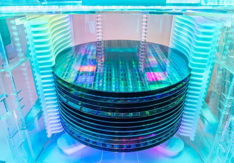
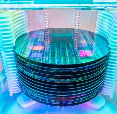
“Silicon wafer stack inside semiconductor fabrication equipment during chip manufacturing process”
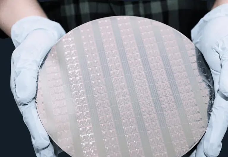
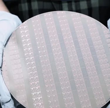
“Compound semiconductor wafer with patterned device structures used in advanced electronics manufacturing”