
Stealth Dicing Explained
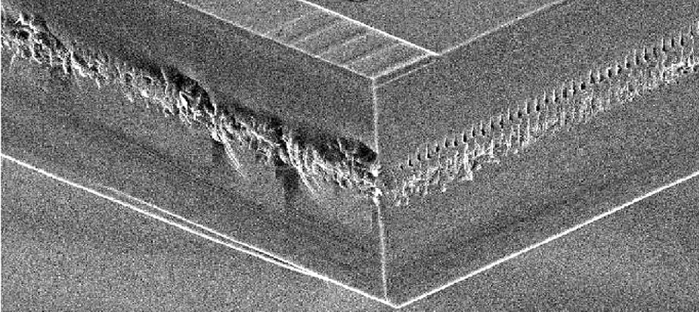
Scanning electron microscope image showing a die edge formed by stealth dicing, highlighting controlled subsurface fracture behavior and edge morphology in semiconductor wafer singulation.
Kiran
1/7/20265 min read
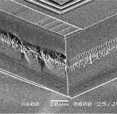
Scanning electron microscope image showing a die edge formed by stealth dicing, highlighting controlled subsurface fracture behavior and edge morphology in semiconductor wafer singulation.
Stealth Dicing Explained: Physics, Process Flow, and Backend Reliability Implications
Introduction
As semiconductor wafers become thinner, more fragile, and more densely integrated, conventional singulation methods increasingly struggle to meet yield and reliability requirements. Mechanical blade dicing introduces vibration and subsurface damage, while laser ablation can generate thermal stress, recast layers, and heat-affected zones. These limitations have driven adoption of alternative singulation techniques designed to minimize direct stress on the wafer surface.
Stealth dicing is one such technique. Rather than cutting entirely through the wafer from the surface, stealth dicing creates a controlled internal fracture plane within the silicon. Final die separation occurs only after internal modification, using minimal external force. This fundamental shift—from surface material removal to subsurface damage engineering—makes stealth dicing particularly attractive for thin wafers, MEMS devices, image sensors, and advanced packaging flows.
This article explains how stealth dicing works, why it behaves differently from conventional laser or blade dicing, and how backend engineers evaluate its impact on yield, edge quality, and long-term reliability.
What Is Stealth Dicing?
Stealth dicing is a laser-based singulation technique that modifies silicon internally without removing surface material. A focused laser beam is directed beneath the wafer surface, where it locally alters the silicon crystal structure. This modified layer acts as a predefined fracture plane.
After the internal layer is created along scribe streets, the wafer is separated using controlled mechanical expansion, tape stretching, or external stress. The wafer cleaves along the internally modified paths rather than being physically cut through from the top surface.
The defining characteristics of stealth dicing are:
Subsurface laser interaction
No open kerf during laser processing
Minimal debris generation
Separation by controlled fracture rather than cutting
How Stealth Dicing Works at a Physical Level
Subsurface Laser Absorption
In stealth dicing, the laser wavelength is selected so that silicon is largely transparent at the surface but absorbs energy at a controlled focal depth. At this focal point, the laser induces localized structural changes such as:
Microvoid formation
Amorphization
High internal stress regions
These changes weaken the silicon along a narrow internal line.
Creation of a Continuous Internal Damage Layer
By scanning the laser along the scribe street, a continuous weakened plane is formed beneath the wafer surface. Importantly:
The wafer surface remains largely intact
No material is ejected
Edge contamination is minimal
This is fundamentally different from ablation-based laser dicing, which removes material from the surface downward.
Controlled Cleavage During Separation
Once the internal damage layer is complete, the wafer is separated by applying mechanical stress—often through tape expansion or bending. The wafer fractures preferentially along the modified plane, producing individual dies.
Because the fracture follows a predefined internal path, separation forces are much lower than in conventional breaking processes.
Key Differences Between Stealth Dicing and Other Dicing Methods
Stealth vs Blade Dicing
Blade dicing removes material mechanically from the surface, generating vibration, debris, and subsurface damage. Stealth dicing:
Eliminates blade contact
Avoids abrasive cutting
Reduces surface chipping
This makes stealth dicing especially valuable for thin wafers where mechanical stiffness is low.
Stealth vs Laser Ablation Dicing
Laser ablation dicing relies on surface heating and material removal. Stealth dicing:
Produces little to no heat-affected zone at the surface
Avoids recast layers
Minimizes thermal gradients
As a result, stealth dicing generally introduces less thermal stress into backend layers.
Stealth vs Plasma Dicing
Plasma dicing chemically removes silicon through masked etching. While plasma dicing produces very clean edges, it requires additional lithography and long cycle times. Stealth dicing offers:
Faster throughput than plasma
Fewer process steps
Lower overall complexity
However, plasma dicing still provides superior edge smoothness in some ultra-high-reliability applications.
Advantages of Stealth Dicing
Reduced Mechanical Stress
Because separation occurs along an internally weakened plane, the force required to singulate dies is much lower than in blade or conventional break processes. This significantly reduces:
Die cracking
Corner fracture
Stress transfer into backend layers
Minimal Debris Generation
Since silicon is not physically removed during laser processing, stealth dicing generates very little particulate contamination. This is especially important for:
MEMS devices with cavities
Image sensors
Devices with exposed passivation
Narrow Effective Kerf Width
Stealth dicing does not require a wide open kerf during laser processing. This allows:
Higher die count per wafer
Tighter scribe street design
Improved silicon utilization
Final separation occurs along a narrow internal plane rather than a mechanically widened cut.
Limitations and Challenges of Stealth Dicing
Dependence on Material Uniformity
Stealth dicing relies on precise control of laser focus depth. Variations in:
Wafer thickness
Local topography
Backside grinding damage
can shift the focal plane and reduce the effectiveness of internal modification.
Sensitivity to Backend Stack Design
Backend layers such as dielectrics, metals, or polymers can influence how stress propagates during separation. In some stacks, cracks may deviate from the intended plane, especially near die edges.
Limited Applicability to Some Materials
Stealth dicing is most effective for crystalline silicon. Its applicability to compound semiconductors or heavily heterogeneous stacks may be limited or require extensive optimization.
Edge Quality and Crack Behavior in Stealth Dicing
Fracture-Defined Edges
Unlike blade or ablation dicing, stealth dicing produces edges defined by controlled fracture rather than material removal. This leads to:
Relatively smooth edges
Lower surface damage
Reduced subsurface crack density
However, because fracture is involved, edge quality can vary depending on crystal orientation and stress distribution.
Crack Propagation Control
When properly optimized, cracks propagate along the intended plane and arrest naturally at the die boundary. If not, cracks can:
Deviate toward active areas
Intersect backend layers
Extend into the die body
This makes separation mechanics just as important as laser parameters.
Stealth Dicing for Thin and Ultra-Thin Wafers
Thin wafers are one of the strongest use cases for stealth dicing. As thickness decreases:
Mechanical cutting becomes increasingly risky
Wafer stiffness drops sharply
Crack tolerance decreases
Stealth dicing minimizes mechanical loading during both laser processing and separation, making it well-suited for wafers below ~100 µm.
Carrier wafers and optimized tape expansion profiles are often used to further control stress during separation.
Applications Where Stealth Dicing Excels
MEMS Devices
MEMS devices benefit from stealth dicing because:
Vibration is minimized
Particle generation is low
Mechanical structures are protected
This reduces risks of fracture, stiction, and calibration drift.
Image Sensors and Optoelectronics
For image sensors, surface integrity and cleanliness are critical. Stealth dicing avoids surface damage and debris that could impact optical performance.
Advanced Packaging Flows
In WLCSP and fan-out flows where RDL extends close to the die edge, stealth dicing reduces the likelihood of:
Line cracking
Passivation delamination
Moisture ingress
Integration Considerations in Backend Manufacturing
Tape and Separation Strategy
Stealth dicing shifts much of the mechanical risk from cutting to separation. Tape selection, adhesion uniformity, and expansion control are therefore critical. Poor tape behavior can negate the benefits of stealth dicing by introducing uncontrolled fracture during separation.
Process Window Definition
Successful stealth dicing requires tight control of:
Laser power and focus depth
Scan overlap and spacing
Separation force and direction
Unlike blade dicing, where parameters are relatively forgiving, stealth dicing windows can be narrow.
Reliability Implications
Stealth dicing generally improves long-term reliability by:
Reducing subsurface damage
Minimizing stress concentration at die edges
Preserving backend layer integrity
However, poorly controlled fracture planes can still create latent crack paths. Reliability validation must therefore include thermal cycling and mechanical stress testing, not just edge inspection.
Backend Engineering Perspective
Stealth dicing is not a drop-in replacement for other dicing methods. It requires coordinated optimization across wafer thinning, tape selection, separation mechanics, and backend stack design.
Silicon Craft Technologies evaluates stealth dicing as part of a holistic backend strategy, assessing how internal fracture behavior interacts with material stacks, wafer thickness, and downstream assembly stress. By integrating singulation decisions early in backend planning, Silicon Craft Technologies helps ensure that stealth dicing delivers its intended yield and reliability benefits.
Conclusion
Stealth dicing represents a fundamental shift in wafer singulation philosophy—from surface material removal to controlled internal fracture. When properly implemented, it offers significant advantages in stress reduction, cleanliness, and thin-wafer capability.
Its success, however, depends on precise control of laser parameters, separation mechanics, and backend integration. As devices continue to scale in fragility and complexity, stealth dicing will remain an important—but carefully engineered—tool in the backend manufacturing toolkit.