
Stress Management in Ultra-Thin Silicon Wafers
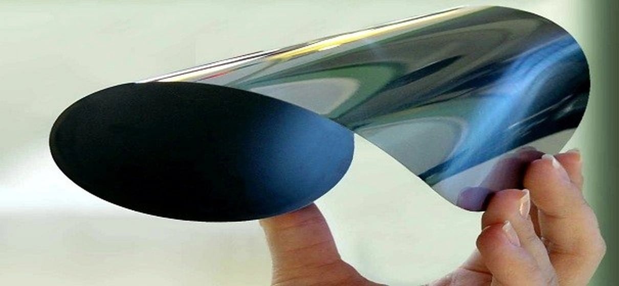
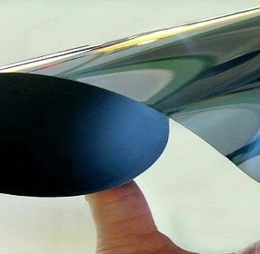
As silicon wafers get thinner, they become harder to handle and easier to damage. This post looks at why stress builds up in ultra-thin wafers, how it shows up as bending or cracking, and the practical ways engineers manage it to keep advanced manufacturing on track.
Kiran
10/2/20253 min read
Introduction
As silicon wafers are thinned below 100 µm for advanced packaging, 3D integration, MEMS, and heterogeneous integration, mechanical stress becomes one of the dominant factors limiting yield and reliability. Ultra-thin wafers are inherently fragile and highly sensitive to residual stress introduced during thinning, thin-film deposition, thermal cycling, and handling. Across academic literature and semiconductor manufacturing reports, stress management is consistently identified as a prerequisite for stable processing of ultra-thin silicon wafers.
Primary Sources of Stress in Ultra-Thin Wafers
Stress in ultra-thin silicon wafers originates from both intrinsic and extrinsic mechanisms. Intrinsic stress is introduced during wafer processing, particularly during mechanical backgrinding, chemical mechanical polishing (CMP), ion implantation, and thin-film deposition. Backgrinding creates subsurface damage and residual stress gradients that become increasingly significant as wafer thickness decreases. Thin films deposited on the wafer—such as metals, dielectrics, or passivation layers—can induce tensile or compressive stress due to mismatches in coefficient of thermal expansion (CTE) and intrinsic film stress.
Extrinsic stress arises during handling and processing. Vacuum chucking, clamping, tape mounting, and thermal mismatch between the wafer and processing fixtures can introduce non-uniform mechanical loads. These stresses often manifest as wafer bow, warp, cracking, or edge chipping, especially during transport or debonding.
Impact of Stress on Manufacturing Yield
Excessive stress in ultra-thin wafers leads to several well-documented failure modes. Wafer bow and warp degrade lithography focus control, alignment accuracy, and bonding uniformity. Localized stress concentrations can cause cracking during debonding, dicing, or thermal cycling. Even when catastrophic failure is avoided, residual stress can drive delamination, die shift, and long-term reliability degradation in packaged devices. As a result, stress control is not only a mechanical concern but also a key enabler of downstream process compatibility.
Temporary Carrier Bonding as a Core Mitigation Strategy
Temporary wafer bonding to a rigid carrier is widely cited as the most effective method for stress management in ultra-thin wafers. In this approach, the device wafer is bonded to a glass or silicon carrier using an adhesive or release layer prior to thinning. The carrier provides mechanical support, suppresses bow, and allows ultra-thin wafers to be processed using standard equipment.
Critical parameters include carrier material selection, adhesive modulus, bond layer thickness uniformity, and debonding method. Mismatch in CTE between the wafer, adhesive, and carrier can reintroduce stress if not carefully controlled. Non-mechanical debonding methods such as UV or laser release are commonly preferred to reduce peel-induced cracking.
Thinning Process Optimization and Stress Relief
The thinning sequence itself plays a major role in residual stress control. Industry-standard practice favors a staged approach: coarse backgrinding for bulk removal, followed by fine backgrinding, then stress-relief steps such as CMP, wet etching, or plasma treatment. CMP and chemical etching remove the damaged surface layer generated during mechanical grinding, significantly reducing residual stress and wafer curvature.
Limiting material removal per step and avoiding aggressive mechanical conditions are consistently recommended. Post-thinning anneals, when carefully temperature-controlled, can further relax residual stress without introducing thermal distortion.
Thin-Film Stack and Thermal Budget Engineering
Thin-film stress management is another critical lever. Symmetric film stacks on the front and back sides of the wafer help balance stress and minimize curvature. When symmetry is not feasible, compensating layers or adjusted deposition parameters can be used to counteract tensile or compressive stress.
Thermal budget control is equally important. High-temperature steps amplify CTE mismatch effects, particularly in bonded wafers. Slower ramp rates, reduced peak temperatures, and grouping of thermally compatible processes are commonly cited strategies to limit thermally induced stress.
Metrology, Monitoring, and Handling Practices
Continuous monitoring is essential for effective stress management. Wafer bow and warp are typically measured using optical or laser-based curvature tools, while residual stress can be inferred using curvature-based models. Tracking stress evolution after each major process step allows engineers to identify and correct dominant stress contributors early in the flow.
Handling practices must also be adapted for ultra-thin wafers. Distributed or low-vacuum chucks, edge support fixtures, and minimized manual handling reduce the risk of localized stress and fracture. Debonding is frequently identified as a high-risk step and requires carefully controlled tooling and process parameters.