
Temporary Wafer Bonding Explained
Explore best practices for wafer cleaning before bumping and bonding to minimize contamination, improve interconnect quality, and enhance backend manufacturing yield.
Kiran
1/5/20265 min read
Temporary wafer bonding has become a foundational enabler for modern semiconductor manufacturing, particularly as devices move toward thinner wafers, higher interconnect density, and more complex 3D and heterogeneous integration schemes. What began as a niche support technique for wafer thinning has evolved into a critical process module that directly influences yield, reliability, and manufacturability in advanced packaging flows.
This article provides a technically grounded explanation of temporary wafer bonding, why it is required, how it is implemented, and the engineering trade-offs that define material and process selection in real production environments.
Why Temporary Wafer Bonding Is Required
As semiconductor devices scale beyond traditional planar architectures, mechanical stability during backend processing becomes a primary constraint rather than a secondary concern. Wafers must often be thinned to tens of microns—or less—to enable through-silicon vias (TSVs), backside redistribution layers, wafer-level packaging, or die stacking. At these thicknesses, a silicon wafer loses sufficient rigidity to withstand conventional handling, lithography, and thermal cycling.
Temporary wafer bonding addresses this limitation by mechanically coupling a device wafer to a rigid carrier wafer. The carrier provides structural support throughout aggressive backend steps such as grinding, polishing, etching, and metallization. Once these processes are complete, the carrier is removed without damaging the device wafer or leaving residues that could compromise downstream assembly.
In effect, temporary bonding decouples mechanical robustness from final device thickness, allowing process engineers to push physical limits without sacrificing yield stability.
Core Elements of a Temporary Wafer Bonding System
At a system level, temporary wafer bonding is defined by three tightly coupled components: the carrier substrate, the bonding interface material, and the debonding method. Each must be selected with the full process flow in mind rather than as isolated choices.
Carrier Wafers
Carrier wafers are typically made from glass or silicon. Glass carriers offer optical transparency, enabling backside alignment during lithography, while silicon carriers provide closely matched thermal expansion behavior. The choice impacts thermal stress, alignment accuracy, and debonding strategy.
Carrier flatness, thickness uniformity, and surface finish are non-negotiable parameters, as any deviation is directly transferred to the device wafer during bonding and subsequent processing.
Bonding Interface Materials
The bonding layer is the functional heart of the system. Common classes include thermoplastic polymers, thermoset adhesives, and inorganic bonding layers. These materials must maintain adhesion across thermal cycles, chemical exposure, and mechanical stress, yet release cleanly during debonding.
No single bonding material is universally optimal. Instead, selection is driven by maximum process temperature, chemical compatibility, required bond strength, and debonding constraints.
Debonding Mechanisms
Debonding must be predictable, controllable, and non-destructive. Mechanical, thermal, laser-assisted, and chemical debonding approaches are all used in production, each with distinct equipment and process implications.
The debonding step is often the highest risk operation in the flow, as it occurs after significant value has already been added to the wafer.
Temporary Wafer Bonding Process Flow
While implementations vary, the high-level process sequence follows a consistent structure.
Surface Preparation
Both device and carrier wafers undergo cleaning and surface conditioning to ensure uniform bonding. Particles, organic residues, or surface roughness can lead to voids, non-uniform stress, or localized delamination.
Bonding
The bonding step applies controlled temperature, pressure, and alignment to form a uniform interface. Process windows are often narrow, particularly for polymer-based systems, where viscosity and flow behavior strongly influence bond uniformity.
Wafer Thinning and Backend Processing
Once bonded, the device wafer can be thinned using grinding and polishing to the target thickness. Subsequent backend processes—such as TSV reveal, backside dielectric deposition, and metallization—are performed with the carrier maintaining mechanical stability.
Debonding and Cleaning
After processing, the carrier is removed using the selected debonding technique. Residual bonding material must be cleaned without attacking device structures, passivation layers, or metals.
Key Temporary Bonding Technologies
Several technology platforms dominate current usage, each optimized for different integration strategies.
Adhesive-Based Temporary Bonding
Adhesive systems are widely adopted due to their process flexibility and relatively low equipment complexity. Thermoplastic adhesives allow debonding through controlled heating, while thermoset systems rely on chemical or mechanical separation.
These approaches are well-suited for wafer thinning and redistribution layer formation but require careful control of outgassing, thermal stability, and residue removal.
Laser-Assisted Debonding
Laser debonding systems use a transparent carrier and a laser-absorbing layer at the interface. A laser pulse locally weakens the bond, enabling clean separation at relatively low thermal load.
This method supports very thin wafers and minimizes mechanical stress, but introduces additional equipment cost and alignment requirements.
Direct and Hybrid Bonding Approaches
Emerging approaches combine adhesive layers with inorganic films or engineered release layers to improve thermal stability and bond uniformity. These hybrid systems are increasingly used in high-temperature or fine-pitch integration schemes.
Engineering Trade-Offs and Failure Modes
Temporary wafer bonding is not a purely mechanical exercise; it is an exercise in managing trade-offs across the entire backend process window.
Thermal Expansion Mismatch
Differences in coefficient of thermal expansion between the device wafer, bonding layer, and carrier can induce bow and stress during thermal cycling. Excessive warpage affects lithography focus, overlay accuracy, and yield.
Chemical Compatibility
Bonding materials must survive exposure to solvents, developers, etchants, and plasma processes. Incompatibility can result in swelling, loss of adhesion, or contamination.
Residue and Contamination Risks
Incomplete removal of bonding materials can interfere with wire bonding, flip-chip assembly, or long-term reliability. Cleaning strategies must be validated as rigorously as the bonding step itself.
Yield Sensitivity
Because temporary bonding occurs early in backend processing, defects introduced at this stage propagate through high-value steps. Process stability and repeatability are therefore critical economic considerations.
Applications Enabled by Temporary Wafer Bonding
Temporary wafer bonding underpins many of the most advanced integration schemes in production today.
In 3D IC integration, it enables TSV formation and wafer stacking at thicknesses that would otherwise be unmanageable. In wafer-level packaging, it supports fan-out redistribution and backside processing. In MEMS and sensor manufacturing, it allows fragile structures to be protected during aggressive etching and release steps.
As heterogeneous integration expands, temporary bonding is increasingly used to manage dissimilar materials and architectures within a single process flow.
Process Optimization and Best Practices
Successful implementation requires early integration of temporary bonding considerations into product and process design. Material selection should be validated against the full thermal and chemical budget. Carrier choice should reflect alignment, warpage, and debonding needs rather than convenience.
Equally important is cross-functional collaboration between process development, equipment engineering, and reliability teams. Temporary bonding is not a standalone module; it is a system-level decision that influences every downstream operation.
Backend Manufacturing Support with Silicon Craft Technologies
Temporary wafer bonding places unique demands on backend manufacturing environments, particularly when transitioning from development to stable production. Process windows are tight, interactions between materials are complex, and failure modes often emerge only after multiple downstream steps.
Silicon Craft Technologies supports these challenges through an engineering-driven approach to backend semiconductor manufacturing and advanced packaging. With capabilities spanning wafer-level and package-level processes, Si-Craft works closely with customers to align temporary bonding strategies with thinning, backside processing, and integration requirements.
This collaborative model enables informed trade-offs between bonding materials, carrier selection, and debonding methods, while maintaining flexibility for prototyping and low-to-medium volume production. By grounding process decisions in manufacturing realities rather than isolated specifications, Silicon Craft Technologies helps ensure that temporary wafer bonding functions as a reliable enabler—not a bottleneck—within advanced semiconductor workflows.
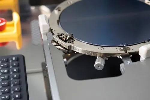
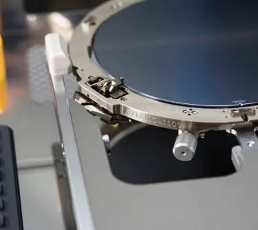
“Close-up of a temporary wafer bonding tool clamping a silicon wafer on a carrier substrate for backend semiconductor manufacturing”