
Wafer Bumping Explained
A clear, in-depth overview of wafer bumping, explaining key processes, materials, and manufacturing considerations that enable flip-chip assembly and advanced semiconductor packaging.
Kiran
1/6/20266 min read
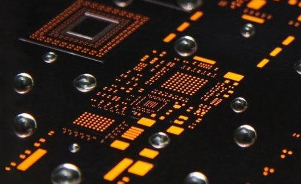
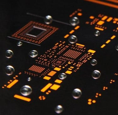
This image illustrates wafer bumping patterns used for flip-chip semiconductor interconnects, highlighting high-density bump arrays that enable advanced packaging and improved electrical performance.
Wafer Bumping Explained: Foundations, Processes, and Manufacturing Considerations
As semiconductor packaging continues to evolve toward higher I/O density, smaller form factors, and improved electrical performance, wafer bumping has become a foundational backend technology. Once considered a niche process reserved for advanced applications, wafer bumping is now widely used across logic, memory, RF, automotive, and high-performance computing devices. Understanding wafer bumping is essential for anyone involved in modern semiconductor manufacturing, packaging design, or backend process integration.
Wafer bumping creates microscopic electrical interconnects directly on the wafer surface, enabling flip-chip assembly and advanced packaging architectures. These bumps replace traditional wire bonds by providing shorter electrical paths, higher interconnect density, and improved thermal performance. However, wafer bumping introduces new process complexities, material interactions, and reliability considerations that must be carefully managed.
This article explains wafer bumping from the ground up, covering why it is used, how it is performed, the major bumping technologies, and the manufacturing challenges that define successful implementation.
What Is Wafer Bumping?
Wafer bumping is a backend semiconductor process in which small conductive bumps are formed on the bond pads of a wafer before singulation. These bumps serve as the electrical and mechanical connection points between the die and the substrate or package during flip-chip assembly.
Unlike wire bonding, where interconnects are created after die attach, wafer bumping prepares the die for face-down mounting. Electrical signals travel directly through the bumps into the package substrate, dramatically shortening signal paths and reducing parasitic resistance and inductance.
Wafer bumping is typically performed at the wafer level, allowing all dies on the wafer to be processed simultaneously. This parallel processing improves throughput and enables tighter control of interconnect geometry and uniformity.
Why Wafer Bumping Is Used
The adoption of wafer bumping is driven by several key performance and integration advantages.
Shorter electrical paths improve signal integrity, making wafer bumping particularly attractive for high-speed and high-frequency devices. Reduced inductance and resistance allow better performance at lower power levels.
Higher I/O density is another major advantage. Because bumps can be placed across the entire die surface rather than only around the perimeter, wafer bumping enables area-array interconnects. This is essential for large, complex chips with thousands of I/O connections.
Thermal performance also benefits. Direct die-to-substrate contact through bumps improves heat dissipation compared to wire-bonded packages, where heat must travel through longer paths.
Finally, wafer bumping supports advanced packaging architectures such as flip-chip BGA, chip-scale packages, fan-out wafer-level packaging, and 2.5D/3D integration.
The Basic Wafer Bumping Process Flow
While specific steps vary depending on the bumping technology, most wafer bumping processes follow a similar high-level flow.
The process begins with wafer preparation, including cleaning and surface conditioning. Bond pads must be free of contaminants and oxides to ensure strong adhesion and reliable electrical contact.
A passivation opening is then created over each pad if necessary. This defines where bumps will be formed and protects surrounding circuitry.
Next, an under-bump metallization (UBM) stack is deposited. The UBM serves multiple purposes: it provides adhesion to the pad, acts as a diffusion barrier, and creates a wettable surface for the bump material.
After UBM formation, the bump material itself is deposited. Depending on the technology, this may involve electroplating, solder paste printing, evaporation, or chemical deposition.
Once bumps are formed, they may undergo reflow to shape them into controlled spheres. Excess materials are removed, and the wafer is inspected before being sent for singulation and assembly.
Under-Bump Metallization and Its Role
Under-bump metallization is a critical component of wafer bumping. Without a properly designed UBM stack, bump reliability and adhesion suffer dramatically.
The UBM typically consists of multiple thin layers, each serving a specific function. An adhesion layer ensures strong bonding to the aluminum or copper pad. A barrier layer prevents diffusion between the pad metal and the bump material. A wetting layer promotes uniform bump formation and attachment.
Common UBM materials include titanium, tungsten, nickel, copper, and combinations thereof. The exact stack design depends on the bump material, pad metallurgy, and reliability requirements.
UBM optimization is often one of the most challenging aspects of wafer bumping because failures may not appear until thermal cycling or long-term operation.
Solder Bumping Explained
Solder bumping is the most widely used wafer bumping technology. It relies on solder alloys to form the interconnect bumps.
In solder bumping, solder is deposited onto the UBM pads and then reflowed to form spherical bumps. Common solder alloys include lead-free compositions such as SAC (tin-silver-copper) and high-lead alloys for specialized applications.
Solder bumping offers good self-alignment during assembly, strong mechanical attachment, and established reliability data. It is widely used in flip-chip BGAs, automotive electronics, and consumer devices.
However, solder bumping faces challenges as bump pitch continues to shrink. At very fine pitches, solder bridging, voiding, and collapse control become difficult.
Copper Pillar Bumping
Copper pillar bumping has emerged as a popular alternative to traditional solder bumps, especially for advanced nodes and fine-pitch designs.
In this approach, a copper column is electroplated onto the UBM, followed by a thin solder cap. The copper pillar provides mechanical height and stiffness, while the solder cap enables attachment to the substrate.
Copper pillars offer better pitch scalability, improved current carrying capacity, and more controlled bump geometry. They are widely used in advanced logic devices, high-performance computing, and mobile processors.
However, copper pillar bumping introduces tighter process control requirements and greater sensitivity to substrate planarity and assembly alignment.
Gold Bumping and Stud Bumping
Gold bumping, often performed using stud bumping techniques, is another wafer bumping method commonly used for lower-volume or specialized applications.
Stud bumping uses modified wire bonding equipment to place gold balls directly onto wafer pads. The wire is then broken, leaving a gold stud attached to the pad.
Gold stud bumping is flexible and does not require photolithography, making it suitable for prototyping, MEMS devices, and RF applications. It is also commonly used for wafer-level testing and temporary interconnects.
The main limitations of gold bumping are lower throughput and higher cost compared to plated bumping methods.
Wafer Bumping for Fan-Out and Wafer-Level Packaging
Wafer bumping plays a central role in fan-out wafer-level packaging (FOWLP) and other advanced wafer-level techniques.
In these architectures, bumped dies are embedded in mold compound and redistributed using redistribution layers (RDLs). Wafer bumping enables high-density interconnects without traditional substrates.
Fan-out packaging benefits from smaller form factors, improved electrical performance, and reduced package height. Wafer bumping accuracy and uniformity are especially critical in these processes because misalignment can cascade into RDL failures.
Manufacturing Challenges in Wafer Bumping
Despite its advantages, wafer bumping introduces several manufacturing challenges that must be addressed through careful process optimization.
Uniformity across the wafer is a major concern. Variations in bump height, diameter, or shape can cause assembly defects, poor coplanarity, and open or shorted connections.
Material interactions between the pad, UBM, bump, and substrate can create reliability risks such as intermetallic growth, cracking, or delamination.
Process complexity is another challenge. Wafer bumping involves multiple thin-film, lithography, and plating steps that must be tightly controlled.
Yield loss in wafer bumping can be expensive because defects affect entire wafers rather than individual dies.
Inspection and Metrology for Wafer Bumping
Inspection plays a crucial role in wafer bumping success. Optical inspection is used to detect missing, deformed, or bridged bumps. X-ray inspection helps identify voids and internal defects.
Metrology tools measure bump height, diameter, and coplanarity to ensure compatibility with downstream assembly processes. Statistical process control is used to monitor trends and detect drift.
Because wafer bumping defects can propagate into assembly failures, early detection is essential.
Reliability Considerations
Reliability testing is critical for wafer-bumped devices. Common tests include thermal cycling, thermal shock, power cycling, and humidity exposure.
Failure modes may include bump cracking, intermetallic embrittlement, UBM delamination, or solder fatigue. Reliability performance depends heavily on material selection, UBM design, and bump geometry.
Processes that appear robust during initial testing may fail under extended stress if wafer bumping is not properly optimized.
Wafer Bumping vs Wire Bonding
Wafer bumping is often compared directly with wire bonding, but the two technologies serve different needs.
Wafer bumping excels in high-I/O, high-performance, and compact designs. Wire bonding remains competitive for cost-sensitive, lower-density, and highly flexible applications.
In many product portfolios, both technologies coexist, with wafer bumping used selectively where its advantages justify the added complexity.
The Future of Wafer Bumping
As semiconductor devices continue to scale and packaging becomes increasingly heterogeneous, wafer bumping will remain a critical enabling technology.
Trends such as smaller pitches, alternative materials, and integration with 3D stacking will drive continued innovation in wafer bumping processes.
Success will depend on deep understanding of materials, tight process control, and close collaboration between design, wafer fabrication, and backend assembly teams.
Conclusion
Wafer bumping is far more than a simple interconnect technique. It is a sophisticated backend process that directly influences electrical performance, mechanical reliability, and package scalability.
Understanding wafer bumping—its purpose, processes, materials, and challenges—is essential for modern semiconductor manufacturing. When implemented and optimized correctly, wafer bumping enables the advanced packaging technologies that define today’s and tomorrow’s electronics.