
Wafer Bumping for Prototyping
An in-depth look at wafer bumping for prototyping, covering process options, materials, inspection, and risk management strategies that support early-stage validation and a smooth transition to production-scale semiconductor packaging.
Kiran
1/6/20265 min read
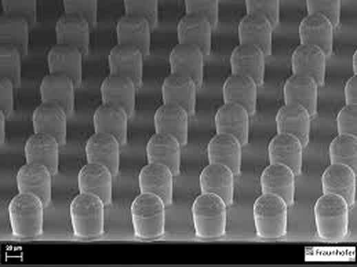
Scanning electron microscope image showing uniform solder bump arrays used in wafer bumping and advanced semiconductor packaging.
Wafer Bumping for Prototyping: Process Flexibility, Risk Control, and Early-Stage Manufacturability
Introduction
Wafer bumping plays a foundational role in advanced semiconductor packaging, enabling electrical, mechanical, and thermal interconnection between the silicon die and downstream substrates or boards. While high-volume wafer bumping is often discussed in the context of yield optimization and cost efficiency, wafer bumping for prototyping presents a distinctly different set of technical priorities and constraints.
In prototyping environments, the objective is not maximum throughput or lowest cost per unit. Instead, success is measured by process flexibility, fast iteration, data quality, and risk reduction ahead of volume ramp. Wafer bumping decisions made during prototyping directly influence downstream assembly behavior, reliability characterization, and the feasibility of future scale-up.
This article examines wafer bumping specifically through the lens of prototyping and early-stage development, exploring process options, material trade-offs, equipment considerations, and common pitfalls. It also explains why prototyping bump flows must be engineered differently from production-optimized flows to avoid misleading results and costly redesigns.
Why Wafer Bumping Is Critical in Prototyping
Early Electrical and Mechanical Validation
Wafer bumping enables realistic electrical and mechanical interfaces during early silicon evaluation. Without bumps, test vehicles are limited to probe-based measurements that do not reflect true interconnect behavior. Bumped wafers allow engineers to evaluate:
Contact resistance and signal integrity
Power delivery performance
Mechanical compliance and stress distribution
Assembly compatibility with target substrates
For advanced nodes and fine-pitch designs, these factors cannot be accurately extrapolated without physical bumps.
Risk Identification Before Volume Commitments
Prototyping bump processes expose integration risks early, when design and process changes are still economically viable. Issues such as bump collapse behavior, coplanarity sensitivity, solder alloy selection, and UBM stack integrity often surface only after physical interconnection is formed.
Identifying these risks during prototyping prevents late-stage surprises that are far more costly once tooling, materials, and supply chains are locked in.
Key Differences Between Prototype and Production Bumping
Flexibility Over Throughput
Production wafer bumping emphasizes stable, high-throughput processes with narrow operating windows. Prototyping, by contrast, requires process flexibility—the ability to change bump pitch, diameter, metallurgy, and stack design across short timeframes and small lot sizes.
Prototype flows often prioritize tool accessibility and recipe tunability over cycle time, accepting lower throughput in exchange for faster learning cycles.
Data Quality Over Yield Optimization
In prototyping, yield metrics are informative rather than definitive. A lower-yield prototype run can still be successful if it generates clear data on failure mechanisms, process sensitivities, and design margins.
This contrasts with production environments, where yield loss directly translates into cost and must be aggressively minimized.
Common Wafer Bumping Technologies for Prototyping
Solder Bump Reflow Processes
Solder bumping remains one of the most common prototyping approaches due to its compatibility with standard flip-chip and WLP assembly flows. Solder can be deposited via electroplating, stencil printing, or solder ball placement, depending on pitch and volume requirements.
For prototyping, electroplated solder offers precise volume control and scalability, while printed solder can be advantageous for rapid iteration at coarser pitches.
Copper Pillar Bumping
Copper pillar bumping is increasingly used in prototyping for advanced nodes and fine-pitch applications. Copper pillars provide controlled standoff height, improved current carrying capability, and reduced solder volume.
In prototyping, copper pillar dimensions, cap metallurgy, and reflow behavior are often varied intentionally to evaluate assembly sensitivity and reliability trade-offs.
Gold Stud Bumping
Gold stud bumping is frequently used for low-volume prototyping and engineering validation due to its minimal tooling requirements and rapid turnaround. It enables early electrical testing without full wafer-level metallization.
However, gold studs are generally unsuitable for production scaling and can mask issues related to solder wetting, collapse, and fatigue behavior.
Materials and Stack Considerations
Under-Bump Metallization (UBM)
UBM stack design is a critical variable in prototyping. Common stacks include combinations of titanium, nickel, copper, and gold, each serving adhesion, barrier, and wetting functions.
In prototyping, UBM thickness and composition may be intentionally varied to study intermetallic formation, adhesion robustness, and electromigration behavior before finalizing a production stack.
Solder Alloy Selection
Prototype bumping often involves evaluating multiple solder alloys to balance melting temperature, mechanical compliance, and reliability. Lead-free alloys dominate modern designs, but alloy composition can significantly affect bump height, collapse uniformity, and fatigue life.
Testing these variables early helps avoid downstream assembly requalification.
Lithography and Patterning Challenges
Feature Definition at Low Volumes
Photolithography in prototyping must support frequent mask changes and small lot sizes. Resist selection, exposure parameters, and development windows may differ from production-optimized settings.
Misalignment or resist profile variation can distort bump geometry, making it difficult to distinguish true design issues from process artifacts if not carefully controlled.
Pattern Density Effects
Even in prototyping, pattern density strongly influences plating uniformity and bump height. Test vehicles that do not represent final layout density can produce misleading results, particularly for copper pillar or fine-pitch solder bumps.
Well-designed prototypes include representative dummy structures to maintain realistic process loading.
Reflow and Thermal Sequencing
Controlled Collapse Behavior
Reflow profiles used in prototyping must be carefully tuned to reflect intended production conditions. Overly aggressive profiles can artificially improve wetting or collapse behavior, masking marginal designs.
Conversely, conservative profiles may exaggerate failure mechanisms that would not occur in volume assembly.
Multiple Reflow Exposure
Prototype devices often experience multiple reflow cycles during evaluation, rework, and board assembly. Understanding how bump structures evolve across repeated thermal exposure is essential for reliable design decisions.
Inspection and Metrology in Prototyping
Height and Coplanarity Measurement
Bump height and coplanarity measurements are particularly important in prototyping, as they directly influence assembly yield and board-level reliability. Non-contact 3D metrology provides insight into process stability and layout sensitivity.
Defect Characterization
Rather than screening out defects, prototyping inspection focuses on defect characterization. Voids, non-wets, and intermetallic anomalies are analyzed to understand root causes and process limits.
This diagnostic mindset differentiates prototyping from production screening.
Common Pitfalls in Prototype Wafer Bumping
Over-Optimizing for Early Success
One of the most common mistakes in prototyping is optimizing the bump process to “look good” rather than to reflect realistic production conditions. This can lead to false confidence and late-stage failures during scale-up.
Ignoring Manufacturability Signals
Prototype results that require excessive process tuning or manual intervention often indicate poor manufacturability. Treating these signals seriously can prevent costly redesigns later.
Using Non-Scalable Techniques
Techniques like gold stud bumping can accelerate early testing but should be transitioned to scalable processes as soon as practical to avoid disconnects between prototype and production behavior.
Transitioning from Prototype to Production
A successful prototyping bump flow is one that transitions smoothly into production with minimal rework. This requires:
Early alignment on target pitch, materials, and stack design
Documentation of process sensitivities and failure modes
Incremental tightening of process windows as design stabilizes
Prototyping should progressively converge toward production reality, not diverge from it.
Backend Manufacturing Support with Silicon Craft Technologies
Wafer bumping for prototyping demands a different mindset than high-volume manufacturing. Flexibility, process transparency, and engineering collaboration are often more valuable than raw throughput or cost efficiency.
Silicon Craft Technologies supports wafer bumping for prototyping through an engineering-driven backend manufacturing approach tailored to early-stage development needs. With experience across solder bumping, copper pillar formation, UBM stack development, and wafer-level inspection, Si-Craft enables rapid iteration without sacrificing technical rigor.
Rather than forcing prototype designs into production-optimized flows prematurely, Silicon Craft Technologies works collaboratively to evaluate bump structures, materials, and process sequences in a controlled, data-rich environment. This approach helps customers identify integration risks early, validate assembly compatibility, and build a clear roadmap toward scalable manufacturing.
By aligning prototyping objectives with long-term manufacturability, Silicon Craft Technologies provides backend support that bridges the gap between early silicon validation and confident production execution.