
Wafer Cleaning Before Bumping & Bonding
Learn how the semiconductor wafer cleaning process removes contaminants, protects device integrity, and improves yield across advanced manufacturing stages.
Kiran
1/5/20265 min read
As advanced packaging technologies such as flip-chip, fan-out wafer-level packaging (FOWLP), 2.5D interposers, and 3D integration continue to scale, wafer surface cleanliness has become a decisive factor in assembly yield and long-term reliability. While front-end fabrication establishes device functionality, back-end processes such as bumping and bonding determine whether that functionality can be reliably translated into a finished package.
Wafer cleaning before bumping and bonding is often underestimated because contamination may not immediately cause visible defects. However, residues left on the wafer surface—organic films, particles, native oxides, or metallic contaminants—can directly degrade solder wetting, bond strength, electrical continuity, and thermal performance. In high-density interconnect schemes, even nanometer-scale contamination can be enough to cause non-wet opens, voids, or early-life failures.
This article examines the role of wafer cleaning prior to bumping and bonding, the types of contamination that must be controlled, and best practices for integrating cleaning steps into backend manufacturing flows.
Why Wafer Cleaning Is Critical Before Bumping and Bonding
Bumping and bonding processes rely on intimate physical and chemical contact between materials. Solder bumps, copper pillars, micro-bumps, and hybrid bonding interfaces all require clean, activated surfaces to achieve uniform wetting and strong metallurgical bonds.
Contamination at this stage can lead to:
Incomplete solder wetting
Weak intermetallic formation
Increased contact resistance
Voids and delamination
Reduced mechanical strength
Latent reliability failures during thermal cycling
Unlike some front-end processes, backend assembly offers limited opportunities for defect correction. Once bumps are formed or dies are bonded, defects caused by poor surface cleanliness are difficult or impossible to repair without scrapping the wafer or package.
Common Sources of Contamination in Backend Manufacturing
Organic Residues
Organic contamination can originate from photoresist residues, temporary bonding adhesives, protective coatings, handling materials, or airborne hydrocarbons. These residues form thin films that inhibit solder wetting and prevent direct metal-to-metal contact during bonding.
Even trace organic films can significantly reduce surface energy, leading to non-uniform bump formation or weak bonds.
Particulate Contamination
Particles introduced during grinding, handling, cleaning, or transport can become embedded on the wafer surface. In bumping processes, particles may cause missing or deformed bumps, while in bonding they can create standoff defects or localized stress points.
As interconnect pitch continues to shrink, the tolerance for particles decreases dramatically.
Native Oxides and Metal Oxidation
Metal surfaces such as copper, nickel, or aluminum readily form native oxides when exposed to air. These oxides act as diffusion barriers and can inhibit solder wetting or direct bonding mechanisms.
While some bonding processes tolerate thin oxide layers, excessive oxidation reduces bond strength and electrical performance.
Chemical Residues
Incomplete removal of cleaning chemistries, etchants, or plating solutions can leave ionic residues that promote corrosion or electromigration. These residues may not cause immediate failure but can significantly reduce long-term reliability.
Cleaning Requirements for Different Bumping Technologies
Solder Bumping
For solder bumping, surface cleanliness directly affects solder wetting and bump uniformity. Oxides on under-bump metallization (UBM) layers must be minimized, and organic residues must be removed to ensure consistent solder spread and intermetallic formation.
Pre-bump cleaning typically focuses on:
Organic residue removal
Particle reduction
Oxide control on metal pads
Copper Pillar and Micro-Bumping
Copper pillar and micro-bump technologies are more sensitive to surface condition due to finer pitch and higher interconnect density. Even small contaminants can disrupt pillar geometry or bonding alignment.
Cleaning steps must be tightly controlled to avoid over-etching or surface roughening, which can affect pillar height uniformity and bonding coplanarity.
Hybrid and Direct Bonding
Hybrid bonding requires near-perfect surface cleanliness and planarity. Organic films, particles, or oxide layers at the bonding interface can prevent atomic-level contact, leading to voids or incomplete bonds.
In these applications, cleaning is often combined with surface activation steps to enhance bonding readiness.
Integration of Cleaning into Backend Process Flows
Timing of Cleaning Steps
Cleaning should be strategically placed to minimize re-contamination. Common insertion points include:
After wafer thinning and debonding
Before UBM deposition
Prior to bump plating or printing
Immediately before bonding
Delays between cleaning and subsequent processing should be minimized, especially when oxide-sensitive metals are involved.
Compatibility with Temporary Bonding
For ultra-thin wafers, cleaning must be compatible with temporary bonding materials and carriers. Aggressive chemistries or high mechanical forces can compromise bond integrity or induce wafer warpage.
Cleaning processes should be validated with the full bonded stack in mind, not just the device wafer.
Cleaning Technologies Used in Backend Manufacturing
Wet Chemical Cleaning
Wet cleaning remains widely used due to its effectiveness in removing organic and ionic contaminants. However, chemical selection must balance cleaning efficiency with material compatibility.
Over-aggressive chemistries can attack metal pads or dielectric layers, while insufficient cleaning leaves residues that affect bonding quality.
Spray and Megasonic Cleaning
Spray-based and megasonic cleaning methods improve particle removal while reducing mechanical contact. These approaches are particularly useful for fragile or ultra-thin wafers where mechanical stress must be minimized.
Process parameters such as power, frequency, and exposure time must be carefully optimized.
Plasma Cleaning
Plasma cleaning is often used for final surface preparation before bonding. It effectively removes organic films and lightly activates surfaces without liquid exposure.
However, plasma processes can modify surface chemistry, and excessive treatment may damage sensitive materials or alter bonding behavior.
Challenges in Cleaning Ultra-Thin Wafers
As wafer thickness decreases, cleaning introduces additional risks. Fluid flow, mechanical agitation, and thermal gradients can deform or fracture thin substrates.
Best practices for ultra-thin wafer cleaning include:
Reduced mechanical force
Uniform fluid distribution
Controlled drying to prevent watermarks and stress
Integration with carrier-based handling
Cleaning processes must be qualified specifically for thin wafer conditions rather than adapted from standard-thickness flows.
Impact of Cleaning on Yield and Reliability
The impact of wafer cleaning is often indirect but substantial. Poor cleaning may not cause immediate assembly failure but can lead to:
Increased early-life failures
Degraded thermal cycling performance
Higher contact resistance over time
Reduced package lifetime
Conversely, well-controlled cleaning processes improve bump uniformity, bonding consistency, and long-term reliability, leading to higher effective yield and lower cost of ownership.
Metrology and Inspection After Cleaning
Cleaning effectiveness should be verified using appropriate inspection and metrology techniques. These may include:
Surface particle inspection
Contact angle measurements
Residue analysis
Electrical test correlation
Relying solely on visual inspection is insufficient for advanced packaging nodes, where defects may be below optical resolution.
Best Practices for Wafer Cleaning Before Bumping & Bonding
Key best practices include:
Matching cleaning chemistry to materials and bonding technology
Minimizing time between cleaning and critical bonding steps
Adapting cleaning methods for ultra-thin wafers
Monitoring contamination trends rather than reacting to yield loss
Treating cleaning as a yield-critical process step
Cleaning should be viewed as an enabling technology rather than a support operation.
Backend Manufacturing Support with Silicon Craft Technologies
Effective wafer cleaning before bumping and bonding requires more than selecting the right chemistry or tool. It demands a holistic understanding of how surface condition, mechanical handling, temporary bonding, and downstream assembly interact across the backend manufacturing flow.
Silicon Craft Technologies supports backend manufacturing by helping customers develop cleaning and surface preparation strategies that align with advanced packaging requirements and real-world production constraints. Through process development, prototyping, and low-to-medium volume manufacturing support, Si-Craft works to identify contamination risks early and integrate cleaning steps that improve yield, bond integrity, and long-term reliability.
By embedding wafer cleaning considerations into backend process design, Silicon Craft Technologies enables more predictable assembly outcomes and supports scalable manufacturing as interconnect density and integration complexity continue to increase.
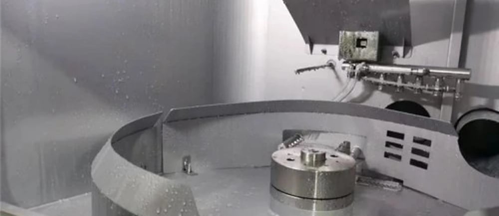
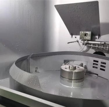
Single-wafer wet cleaning system used for semiconductor wafer cleaning before bumping and bonding”