
What Is Wire Bonding? A Complete Guide to Principles, Materials, and Processes
A detailed technical guide explaining what wire bonding is, why it remains the industry’s dominant interconnect method, and how materials, processes, and bonding techniques shape semiconductor packaging performance. This article covers wire bonding principles, major bonding types, step-by-step process flow, quality factors, reliability concerns, and future technology trends—ideal for engineers, manufacturers, and anyone seeking a deeper understanding of modern microelectronics assembly.
10/2/202518 min read
Introduction: What Is Wire Bonding and Why It Matters
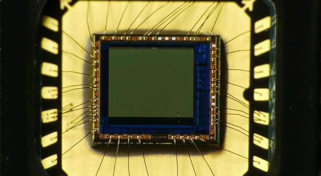
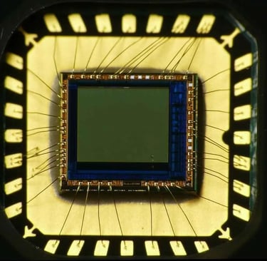
Wire bonding is the foundational interconnect method used to electrically link a semiconductor die to its package, substrate, or lead frame. Despite the rise of advanced packaging technologies, it remains the most widely deployed technique in the industry—powering everything from low-cost microcontrollers to high-reliability aerospace sensors. The process itself is deceptively simple: a fine metallic wire is bonded between the die’s bonding pads and the package terminals. But underneath that simplicity lies a blend of precision mechanics, controlled ultrasonics, carefully tuned metallurgy, and decades of optimization.
The enduring relevance of wire bonding comes from its adaptability. It supports a broad range of materials, package types, device geometries, and performance requirements. Whether the application demands high robustness for automotive electronics, tight bonding pitches for compact consumer ICs, or stable performance under harsh environmental conditions, wire bonding offers a flexible and cost-effective solution. Even as semiconductor scaling accelerates and packaging architectures evolve, wire bonding continues to serve as the workhorse interconnect technology across the global microelectronics supply chain.
Its dominance is not just historical—manufacturers rely on it because it delivers repeatable quality, accommodates rapid prototyping needs, and integrates smoothly into high-volume production environments. In short, wire bonding remains indispensable because it balances performance, manufacturability, and economic efficiency better than almost any alternative.
Why Wire Bonding Remains the Industry Standard
Wire bonding has retained its position as the most widely adopted chip-to-package interconnect method for one primary reason: it consistently delivers the best balance of reliability, flexibility, and cost across an exceptionally wide spectrum of semiconductor applications. Even as advanced packaging technologies gain traction, wire bonding continues to dominate because it solves practical manufacturing challenges in ways that alternative methods often cannot.
Its greatest advantage is versatility. Wire bonding supports a broad range of die materials, metallizations, bonding pad layouts, and package platforms—from traditional lead-frame packages to ceramic modules, power electronics, RF devices, and high-density assemblies. Manufacturers can choose from gold, copper, aluminum, or alloy wires, allowing the process to be optimized for cost, thermal performance, mechanical strength, or long-term reliability. This flexibility is a major reason why the technique remains indispensable in industries such as automotive, industrial automation, power management, and aerospace, where device diversity is extremely high.
Cost efficiency is another powerful driver. Wire bonding is significantly less expensive to set up and operate compared to alternatives like flip-chip bumping or wafer-level redistribution. It supports incremental scaling—engineers can rapidly adjust bond parameters, tooling, and wire types without reengineering an entire package design. This makes it ideal for low- and medium-volume production, ASICs, prototyping, and product families with frequent design updates.
From a reliability standpoint, decades of refinement have made wire bonding exceptionally stable. Process parameters can be tightly controlled, and inspection methods are well developed. Bonding equipment has matured to the point where automated systems can produce millions of bonds per day with consistent loop geometry, bond strength, and alignment accuracy. For high-reliability sectors, the predictability of wire bonding is a critical advantage.
Finally, the method scales gracefully across device generations. As dies become thinner, packages shrink, and power densities rise, bonding tools, wires, and process techniques have evolved in parallel. Innovations such as fine-pitch wedge bonding, low-loop wire architectures, advanced copper bonding, and ultrasonic energy optimization ensure wire bonding remains competitive even in demanding next-generation applications.
In summary, wire bonding continues to thrive because it adapts—materials, equipment, and processes can be tuned to fit virtually any device requirement while maintaining an attractive cost structure and proven reliability. Few interconnect technologies offer this combination of maturity and flexibility.
Materials Used in Wire Bonding
The choice of bonding wire is one of the most influential factors in determining bond quality, long-term reliability, and overall package performance. Different materials exhibit distinct electrical, mechanical, and metallurgical behaviors, and the selection process often balances cost, thermal requirements, operating conditions, and compatibility with die and substrate metallization. While gold dominated the industry for decades, modern manufacturing now supports a broader set of materials tailored to diverse semiconductor applications.
3.1 Gold Wire (Au) — The Traditional Benchmark
Gold remains the most widely recognized wire bonding material due to its excellent softness, corrosion resistance, and predictable bonding behavior. It forms stable intermetallics with aluminum pads and maintains reliability across a wide range of temperatures. Its ductility also enables very fine and controlled loop geometries, making it suitable for high-density, fine-pitch applications and many mainstream IC packages.
Advantages:
Exceptional bond consistency and low bonding force requirements
High corrosion and oxidation resistance
Excellent electrical stability
Ideal for thermosonic ball bonding
Limitations:
Significantly higher cost
Less suitable for high-current or high-temperature power applications
Susceptible to purple plague (Au–Al intermetallic embrittlement) under certain conditions
Despite cost pressures, gold remains prevalent in optical devices, RF modules, smartphones, and sectors where predictable performance outweighs material price.
Copper Wire (Cu) — The Modern Cost-Performance Leader
Copper has emerged as the dominant alternative to gold due to its lower cost and superior electrical and thermal conductivity. It offers higher mechanical strength and better electromigration resistance, making it attractive for power devices, automotive electronics, and high-performance ICs. However, copper requires more controlled processing due to its hardness and susceptibility to oxidation.
Advantages:
Much lower cost than gold
Higher tensile strength and loop stability
Excellent conductivity and heat dissipation
Better long-term reliability in high-current paths
Challenges:
Requires inert or forming-gas environments to prevent oxidation
Higher bonding force can stress fragile dies
Tool and capillary wear occurs more quickly
Alumina pad damage risk is higher if parameters aren’t controlled
Variants such as palladium-coated copper (PCC wire) improve oxidation resistance and bonding stability, enabling copper’s use in increasingly fine-pitch applications.
Aluminum Wire (Al) — The Standard for Power and Wedge Bonding
Aluminum wire is commonly used for wedge bonding, particularly in high-power modules, discrete power semiconductors, and microwave devices. Its oxide layer forms naturally and is stable, making aluminum suitable for harsh or high-temperature environments. Aluminum ribbon and thick wire are also widely used in automotive and industrial applications requiring large cross-section bonding.
Advantages:
Ideal for ultrasonic wedge bonding
Stable at elevated temperatures
Compatible with thick-wire and ribbon bonding for power electronics
Excellent mismatch tolerance in thermal cycling environments
Limitations:
Lower conductivity than copper
Not suitable for ultrafine pitches
Aluminum pads can be damaged with improper ultrasonic energy
Aluminum’s strength, thermal stability, and wedge-bond compatibility make it essential for SiC and GaN power modules, high-power LEDs, and RF amplifiers.
Specialty Materials and Advanced Variants
As device requirements evolve, several specialized bonding wires have gained traction:
Palladium-Coated Copper (PCC)
Enhances oxidation resistance
Reduces tool wear and improves bondability
Expands copper’s usability in sensitive device structures
Silver Alloy Wires
Used in niche applications requiring high reflectivity or specific metallurgical properties
Good for optical, sensor, and hybrid module assemblies
Fine-Pitch Copper Alloys
Tailored for miniaturized ICs and advanced packaging
Improved softness and controlled hardness for reduced die stress
These advanced materials give manufacturers more flexibility to optimize bonding performance while meeting the thermal, mechanical, and cost constraints of next-generation electronics.
Summary of Material Selection Logic
Choosing the right bonding wire involves evaluating:
Electrical and thermal performance needs
Mechanical stresses and loop geometry requirements
Environmental exposure and reliability expectations
Die metallization compatibility
Cost and production volume
Package type (e.g., fine-pitch IC vs high-power module)
In practice, gold offers unmatched ease and consistency, copper delivers the best cost-to-performance ratio, and aluminum remains indispensable in power and wedge-bond applications. Together, these materials form the backbone of the wire bonding ecosystem, ensuring that the process can accommodate everything from delicate MEMS sensors to high-current SiC power devices.
Types of Wire Bonding Techniques
Wire bonding encompasses several bonding methods, each optimized for specific materials, device architectures, and performance requirements. Although the industry has standardized around thermosonic ball bonding and ultrasonic wedge bonding, the underlying techniques differ significantly in how they generate energy, form metallurgical bonds, and accommodate package designs. Understanding these methods is essential for selecting the appropriate process for a given semiconductor device.
4.1 Thermosonic Ball Bonding
Therosonic ball bonding is the most widely used technique in semiconductor packaging, especially for high-volume integrated circuits. It combines heat, ultrasonic energy, and pressure to form strong, consistent bonds using primarily gold or copper wire.
How It Works
The wire feeds through a capillary tool.
An electronic flame-off (EFO) process melts the wire tip, creating a spherical free-air ball (FAB).
The capillary presses the ball onto the bond pad while applying ultrasonic energy.
The combination of force, vibration, and heat forms a robust first (ball) bond.
The tool then forms a controlled loop shape before creating the second (stitch) bond.
Key Characteristics
Ideal for fine-pitch, high-density devices.
Supports very small wire diameters and precise loop geometries.
Offers high throughput suitable for mass production.
Common Applications
CMOS and logic ICs
Memory devices
Mobile and consumer electronics
RF and mixed-signal ICs
Ball bonding remains popular because it delivers a repeatable, efficient process that balances speed, accuracy, and bond integrity.
4.2 Ultrasonic Wedge Bonding
Wedge bonding relies primarily on ultrasonic energy and pressure, often at lower temperatures than ball bonding. It is the preferred technique for aluminum wire, though copper wedge bonding is increasingly common.
How It Works
The wire is fed at a shallow angle through a wedge-shaped bonding tool.
The tool presses the wire onto the pad while ultrasonic vibrations scrub the surfaces together, forming the bond through interdiffusion and frictional energy.
The tool lifts, forms the loop, rotates as needed, and makes the second wedge bond.
Key Characteristics
Excellent for fine-pitch and fine-line applications.
Produces low-loop profiles ideal for stacked-die architectures.
Suitable for thick-wire bonding used in power electronics.
Common Applications
Automotive power modules
SiC and GaN power devices
RF modules and microwave circuits
MEMS devices
Hybrid microelectronics
Because wedge bonding can operate at lower temperatures, it is beneficial for heat-sensitive substrates and devices.
Thermocompression Bonding
Thermocompression bonding is an older but still relevant technique that uses elevated temperature and pressure without ultrasonic energy. It is typically applied to gold wires or ribbons and is especially useful when bonding to fragile metallizations or when ultrasonic-induced stress must be avoided.
How It Works
The bonding tool presses the wire into the pad at high temperature.
The bond forms through solid-state diffusion and metallurgical deformation.
Characteristics
Lower mechanical vibration makes it suitable for delicate materials.
Strong, stable intermetallics are formed.
Slower and less flexible than thermosonic or wedge bonding.
Applications
Military and aerospace-grade packages
Some ceramic substrates
Specialty hybrid modules
While less common in modern mass production, thermocompression remains valuable for niche assemblies requiring precise metallurgical control.
4.4 Advanced and Specialized Bonding Variants
As device architectures evolve, hybrid and specialized bonding techniques have emerged to support high-density packaging, advanced power modules, and novel materials.
Stitch Bonding
Uses multiple fine bonds in place of a single ball bond.
Helpful in optimizing loop profiles and reducing stress in compact layouts.
Low-Loop / Ultra-Low-Loop Bonding
Reduces loop height significantly to accommodate stacked dies.
Essential for multichip modules and 3D packaging.
Ribbon Bonding
Utilizes flat ribbons instead of round wire.
Provides lower inductance and better current-carrying capacity.
Widely used in power modules and RF devices.
Copper Fine-Pitch Ball Bonding
Developed to extend copper usage into ultra-miniaturized ICs.
Requires advanced capillary designs and optimized EFO parameters.
These variants reflect wire bonding’s adaptability—continually evolving to match the demands of smaller, faster, and more thermally intense semiconductor devices.
Summary of Technique Selection
Choosing the right bonding method depends on:
Wire material (Au → ball bonding; Al → wedge bonding)
Pitch and loop height requirements
Thermal budget and substrate sensitivity
Electrical and mechanical stresses
Package and die architecture
Production volume and cost constraints
Each technique offers a specific balance of precision, strength, and manufacturability, ensuring wire bonding remains viable across an exceptionally broad range of applications.
5.Step-by-Step Wire Bonding Process
Wire bonding may appear straightforward at a glance, but the actual process involves a carefully choreographed sequence of mechanical motions, thermal control, ultrasonic energy delivery, and real-time feedback from the bonding equipment. Each stage is designed to create strong, repeatable, and contamination-free interconnects while minimizing stress on the die and substrate. Below is a detailed walkthrough of the typical flow used in modern semiconductor assembly.
5.1 Surface Preparation and Die Positioning
Before any bonding occurs, the die must be properly attached and the bonding surfaces thoroughly cleaned.
Key steps include:
Die attach: The die is mounted to the package or substrate using epoxy, solder, or eutectic bonding.
Cure or reflow: Ensures mechanical stability and flatness.
Pad cleaning: Plasma cleaning, mild etching, or solvent cleaning removes oxides and organic residues.
Contaminants such as moisture, polymer residues, or oxide films can prevent proper intermetallic formation, making this stage foundational to bond reliability.
5.2 Wire Feeding and Tool Alignment
The bonding tool—either a capillary (ball bonding) or wedge tool (wedge bonding)—must be precisely aligned with the bond pads.
Alignment considerations:
Vision systems locate pads and adjust X/Y/Z positions.
Auto-teach algorithms refine tool height, touchdown force, and approach angles.
Wire threading ensures proper feed tension and loop control.
Any error here directly affects positional accuracy and the geometry of the final loop.
5.3 First Bond Formation (Ball or Wedge Bond)
This is the most critical point in the process, where metallurgical bonding occurs.
For thermosonic ball bonding:
An electronic flame-off (EFO) creates a free-air ball at the wire tip.
The capillary descends onto the bond pad.
Heat, pressure, and ultrasonic vibration combine to deform the ball and initiate intermetallic growth.
For ultrasonic wedge bonding:
The wedge tool applies pressure while ultrasonic energy scrubs the wire against the pad surface.
Diffusion and frictional heating form the metallurgical bond.
Perfecting first-bond integrity is essential for ensuring long-term reliability, especially in high-temperature or high-vibration environments.
5.4 Loop Formation and Wire Control
After the first bond forms, the tool lifts and moves to shape the wire loop. Loop architecture is engineered to minimize stress, avoid sagging, and optimize electrical performance.
Common loop types:
Standard loop
Low-loop
Ultra-low-loop
Reverse loop
S-loop for stacked dies
Loop formation depends on parameters such as:
Wire length
Tool motion path
Ultrasonic energy taper
Wire stiffness and material
Capillary geometry
Modern bonding systems adapt loop profiles dynamically to compensate for die tilt, pad height differences, or thermal expansion.
5.5 Second Bond (Stitch or Wedge Bond)
The tool secures the wire’s end to the second pad or lead finger. This is typically a stitch bond in ball bonding or another wedge bond in wedge processes.
Key considerations:
Lower ultrasonic energy than the first bond
Controlled deformation to prevent pad damage
Avoiding heel cracks or cratering beneath the pad
Proper parameter tuning ensures uniformity across hundreds or thousands of bonds per device.
5.6 Wire Tail Formation and Termination
When the second bond is complete, the tool lifts and breaks the wire by pulling upward in a controlled motion. A short tail remains, which becomes the starting point for the next bond cycle.
A stable tail length is crucial for:
Consistent free-air ball (FAB) formation
Predictable loop heights
Machine throughput and yield
Tail control is one of the most refined aspects of wire bonding equipment design.
5.7 Bond Inspection and In-Process Quality Control
Inspection ensures that every bond meets strength, geometry, and metallurgical criteria. Depending on production volume and device criticality, this may include:
Optical inspection (loop height, alignment, deformation)
Shear testing (ball shear strength)
Pull testing (wire tensile strength and bond integrity)
Real-time monitoring (ultrasonic signature, bond force profiles)
Automated inline inspection systems are widely used in high-volume manufacturing.
5.8 Post-Bond Processing
Once bonding is complete, the device may undergo:
Encapsulation or molding
Underfill application
Thermal curing
Environmental stabilization
These steps protect the wire bonds from mechanical stress, contamination, and thermal cycling during the component’s operational lifetime.
Process Summary
The wire bonding process is a balance of precision mechanics, material science, and automated control. From the first bond to the final inspection, every action must be executed with high repeatability to ensure electrical integrity and long-term reliability. Even a slight deviation—excessive force, insufficient ultrasonic energy, contamination, or misalignment—can lead to defects that compromise device performance.
6.Applications of Wire Bonding Across Industries
6.1 Consumer Electronics
Wire bonding is extensively used in consumer electronics, including microcontrollers, power management ICs, RF components, and memory devices. High-volume manufacturing environments benefit from the speed and maturity of thermosonic ball bonding, which supports fine-pitch designs and compact packages common in smartphones, wearables, and home electronics. The process enables manufacturers to achieve a strong balance between performance, yield, and cost efficiency while maintaining consistent bond quality.
6.2 Automotive Electronics
The automotive sector relies heavily on wire bonding for its robustness and long-term reliability. Devices such as engine control units, sensors, power modules, and safety systems must operate under extreme temperature cycling, vibration, and humidity. Aluminum and copper wire bonding—often using wedge or thick-wire techniques—are favored due to their mechanical strength and thermal stability. With the growth of electric vehicles, wire bonding remains essential for high-current interconnects in power inverters and battery management systems.
6.3 Industrial and Power Electronics
In industrial and power applications, wire bonding is critical for managing high voltages and large current loads. Power MOSFETs, IGBTs, and wide-bandgap devices such as SiC and GaN depend on aluminum wire or ribbon bonding to achieve low electrical resistance and efficient heat dissipation. These applications prioritize electrical performance and mechanical durability over ultra-fine pitch, making wire bonding a well-matched solution.
6.4 Medical and Aerospace Applications
Medical and aerospace electronics place stringent demands on reliability, traceability, and service lifetime. Wire bonding is widely used in implantable medical devices, diagnostic equipment, satellites, and avionics systems, where failure is not an option. Gold wire bonding and tightly controlled process parameters are commonly selected to meet regulatory standards and ensure stable performance in harsh or mission-critical environments.
6.5 MEMS and Sensor Devices
Wire bonding plays a key role in MEMS and sensor packaging, where delicate microstructures and non-standard substrates such as glass or ceramics are common. Low-force bonding techniques, precise alignment, and carefully controlled loop profiles are essential to prevent mechanical damage. In many MEMS designs, wire bonding remains the most practical and flexible interconnect solution.
6.6 Optoelectronic Devices
In optoelectronics—including photodiodes, LEDs, laser drivers, and optical sensors—wire bonding provides reliable electrical connections without obstructing optical paths. Gold wire is frequently used for its corrosion resistance and compatibility with optical materials. Loop geometry is often customized to minimize electromagnetic interference and avoid shadowing in sensitive optical assemblies.
7 — Key Factors Affecting Wire Bond Quality
Achieving reliable wire bonds requires more than selecting the right bonding method or wire material. Bond quality is the result of multiple interdependent parameters that must be carefully balanced and controlled throughout the process. Variations in force, energy, temperature, or surface condition can introduce defects that may not be immediately visible but can compromise long-term performance and reliability. The following factors are central to consistent, high-quality wire bonding.
7.1 Bond Force
Bond force determines how much mechanical pressure is applied during bond formation and directly influences bond strength and pad integrity. If the force is too low, the wire may not deform sufficiently to create a stable metallurgical bond, leading to weak adhesion or non-stick bonds. Excessive force, however, can damage pad metallization, cause cratering in the silicon beneath the pad, or introduce residual mechanical stress.
Proper bond force depends on factors such as wire material, wire diameter, pad metallization, and die thickness. Fine-tuning this parameter is essential for balancing bond strength against the risk of substrate damage.
7.2 Ultrasonic Energy
Ultrasonic energy enables interfacial scrubbing between the wire and bond pad, helping to break down surface oxides and promote atomic diffusion. Insufficient ultrasonic energy can result in incomplete bonding or poor intermetallic formation, while excessive energy may erode pad material, distort wire geometry, or introduce microcracks.
Ultrasonic settings must be matched to the wire material and bonding technique, and are often adjusted dynamically by modern bonding equipment to maintain consistency across all bonds.
7.3 Bonding Temperature
Bonding temperature influences wire softness, intermetallic growth rates, and overall bond stability. Elevated temperatures generally improve bondability but can accelerate undesirable metallurgical reactions or increase thermally induced stress within the device. Lower-temperature processes are often selected for thin dies or temperature-sensitive substrates.
Stable and uniform temperature control across the bonding platform is critical, as temperature variation can lead to inconsistent bond strength and geometry.
7.4 Wire Material and Diameter
Wire material and diameter play a major role in both electrical performance and mechanical durability. Fine-diameter wires support high-density layouts and small pad pitches but are more susceptible to deformation and fatigue. Thicker wires provide higher current-carrying capability and improved mechanical robustness but require higher bonding forces and larger pad areas.
Selecting the appropriate wire involves balancing electrical requirements, mechanical reliability, and package design constraints.
7.5 Pad Metallization and Surface Condition
The composition and cleanliness of the bond pad are fundamental to bond reliability. Oxidation, contamination, or inconsistent metallization thickness can inhibit proper intermetallic formation and lead to variable bond strength.
Common pad materials include aluminum, copper, and nickel-based finishes, each requiring specific bonding parameters. Effective surface preparation—such as plasma cleaning or mild chemical treatment—significantly improves bond yield and consistency.
7.6 Loop Geometry and Wire Routing
Loop geometry affects both mechanical robustness and electrical behavior. Excessively high loops are more vulnerable to vibration, wire sweep during molding, and fatigue failure, while overly low loops increase stress concentration at the wire heel and raise the risk of shorting.
Precise loop control is particularly important in stacked-die packages and compact assemblies where vertical clearance is limited and mechanical tolerances are tight.
7.7 Process and Environmental Stability
Consistent bond quality depends on maintaining stable process conditions over time. Variations in humidity, airborne contamination, equipment calibration, or vibration can introduce subtle inconsistencies that degrade yield and reliability. Copper wire bonding is especially sensitive to oxidation and often requires controlled or inert gas environments.
Long-term bonding performance relies on disciplined process control, routine equipment maintenance, and well-managed cleanroom conditions.
Process Summary
Wire bond quality is the cumulative result of mechanical, thermal, material, and environmental control. Each parameter must be optimized not in isolation, but as part of an integrated process window. When properly managed, these factors enable wire bonding to deliver highly reliable interconnects across a wide range of semiconductor applications.
8 — Common Wire Bond Failures and Reliability Considerations
Even with well-optimized bonding parameters, wire bonds can fail due to mechanical stress, thermal cycling, material interactions, or environmental exposure. Some failures are detected immediately during inspection, while others develop gradually and only appear after extended operation. Understanding these failure mechanisms is essential for improving yield, reliability, and long-term device performance.
8.1 Non-Stick on Pad (NSOP)
Non-stick on pad occurs when the wire fails to adhere properly to the bond pad during bond formation. This defect is often observed during initial bonding but may also appear intermittently in production.
Common causes include:
• Insufficient bond force
• Insufficient ultrasonic energy
• Oxidized or contaminated bond pads
• Incompatible pad metallization
• Worn, damaged, or misaligned bonding tools
Addressing NSOP typically involves parameter optimization, improved surface preparation, and regular tool maintenance.
8.2 Bond Lift-Off
Bond lift-off refers to the separation of the bonded wire from the pad after initial attachment, either during subsequent assembly steps or during device operation.
Contributing factors include:
• Weak or incomplete intermetallic formation
• Thermal expansion mismatch between wire and pad materials
• Mechanical stress during molding or encapsulation
• Improper loop geometry causing stress at the bond interface
This failure mode is particularly critical in applications exposed to high temperatures or sustained vibration.
8.3 Heel Cracking
Heel cracking occurs near the transition between the bonded region and the wire loop, commonly referred to as the wire heel. It is typically a fatigue-driven failure that develops over time rather than immediately after bonding.
Typical causes include:
• Excessive loop height
• Sharp loop angles
• High thermal or mechanical cycling
• Over-deformation during the second bond
• Use of overly hard wire materials
Careful loop design and controlled bonding deformation are key to reducing heel crack risk.
8.4 Pad Cratering
Pad cratering is a mechanical failure in which cracks form in the silicon substrate beneath the bond pad, often without immediate visual indicators.
Factors contributing to cratering include:
• Excessive bonding force
• Aggressive ultrasonic energy settings
• Thin die structures
• Weak or brittle dielectric layers beneath pads
• Inadequate die support during bonding
Cratering may result in latent electrical failures that appear later in reliability testing or field use.
8.5 Intermetallic Growth and Metallurgical Degradation
Intermetallic compounds naturally form between the wire and pad materials during bonding. While necessary for bond formation, excessive growth can lead to brittleness and increased electrical resistance.
Key influences include:
• Prolonged exposure to elevated temperatures
• Incompatible wire–pad material combinations
• Moisture ingress and corrosive environments
• Extended device lifetime requirements
This mechanism is especially relevant in gold–aluminum systems and high-temperature applications.
8.6 Corrosion and Environmental Damage
Environmental exposure can degrade wire bonds through corrosion, oxidation, or chemical attack, particularly in harsh operating conditions.
Risk factors include:
• High humidity or moisture ingress
• Residual halides from molding compounds
• Inadequate encapsulation or sealing
• Use of oxidation-prone materials such as copper
Protective packaging and controlled environments are essential for mitigating these risks.
Reliability Summary
Wire bond reliability depends not only on initial bond quality but also on how the interconnect responds to mechanical, thermal, and environmental stress over time. Many failure modes can be mitigated through proper material selection, optimized bonding parameters, and robust inspection strategies. A clear understanding of these mechanisms allows manufacturers to design wire bonding processes that deliver consistent performance throughout a device’s intended lifetime.
9 — Emerging Trends and Future Directions in Wire Bonding
Although wire bonding is a mature technology, it continues to evolve in response to increasing device complexity, higher power densities, and more demanding reliability requirements. Rather than being replaced outright, wire bonding is being refined through new materials, tighter process control, and advanced equipment capabilities. These developments ensure that wire bonding remains relevant alongside newer interconnect technologies.
9.1 Transition from Gold to Copper-Based Bonding
One of the most significant trends in wire bonding is the industry-wide shift from gold to copper and copper-based alloy wires. This transition is driven by cost pressures and the superior electrical and thermal performance of copper.
Key drivers include:
• Rising gold material costs
• Improved current-carrying capability of copper
• Better electromigration resistance
• Increased adoption of palladium-coated copper (PCC) wires
Advances in capillary design, surface treatments, and inert gas environments have helped overcome copper’s oxidation challenges, enabling its use in increasingly fine-pitch applications.
9.2 Fine-Pitch and Ultra-Fine-Pitch Bonding
As semiconductor devices continue to shrink, wire bonding processes are being pushed to support finer pad pitches and smaller wire diameters without sacrificing reliability.
Key developments include:
• Improved wire alloys with controlled hardness
• Advanced capillary and wedge tool geometries
• Enhanced vision and alignment systems
• Tighter control of ultrasonic energy and bond force
These improvements allow wire bonding to remain viable in compact packages and high-density IC designs.
9.3 Advanced Loop Control and 3D Packaging Support
Modern wire bonding systems now offer sophisticated loop control capabilities that support stacked-die, multi-chip, and three-dimensional packaging architectures.
Key advancements include:
• Ultra-low and programmable loop profiles
• Reverse and S-loop configurations
• Real-time compensation for die tilt and height variation
• Reduced wire sweep during encapsulation
These features enable wire bonding to adapt to increasingly complex package geometries.
9.4 Automation, Data Monitoring, and Smart Bonding Systems
Automation and data-driven process control are transforming wire bonding from a purely mechanical operation into an intelligent manufacturing process.
Emerging capabilities include:
• Real-time monitoring of bond force and ultrasonic signatures
• Closed-loop process adjustment
• Predictive maintenance based on tool wear data
• Integration with factory-level quality and traceability systems
These technologies improve yield, reduce downtime, and enhance long-term process stability.
9.5 High-Power and Wide-Bandgap Device Integration
The rapid growth of SiC and GaN devices for power electronics is driving renewed innovation in wire bonding, particularly in thick-wire and ribbon bonding techniques.
Key focus areas include:
• Aluminum and copper ribbon bonding
• Enhanced thermal and current-handling capability
• Improved fatigue resistance under thermal cycling
• Lower inductance interconnect designs
Wire bonding remains a critical interconnect solution for high-power modules where robustness and electrical performance are paramount.
Future Outlook
Rather than being displaced, wire bonding is evolving to meet the demands of next-generation semiconductor devices. Through material innovation, tighter process control, and smarter equipment, wire bonding continues to offer a compelling balance of cost, flexibility, and reliability. As packaging technologies diversify, wire bonding will remain an essential tool in the semiconductor assembly landscape.
SECTION 10 — Conclusion and Key Takeaways
Wire bonding remains one of the most established and widely used interconnect technologies in semiconductor packaging, not because it is static, but because it continues to adapt. Its strength lies in a unique combination of process maturity, material flexibility, and cost efficiency that few alternatives can match. From fine-pitch consumer ICs to high-power automotive modules and mission-critical aerospace devices, wire bonding continues to deliver reliable electrical connections across a diverse range of applications.
Throughout this article, we have explored the fundamental principles of wire bonding, examined the materials and bonding techniques involved, and walked through the process steps that govern bond formation. We also highlighted the key factors that influence bond quality, common failure mechanisms, and the technological trends shaping the future of wire bonding. Together, these elements underscore why wire bonding remains a cornerstone of modern semiconductor assembly.
As packaging requirements become more complex, wire bonding will continue to coexist with newer interconnect technologies, offering a proven, adaptable, and economically viable solution. When properly designed and controlled, wire bonding delivers long-term reliability, scalable manufacturing, and consistent performance—making it an indispensable part of the semiconductor industry.