
Wire Bonding for MEMS Devices
A technical overview of wire bonding for MEMS devices, exploring packaging challenges, material choices, process control, and reliability considerations needed to protect sensitive MEMS structures during assembly.
Kiran
1/6/20265 min read
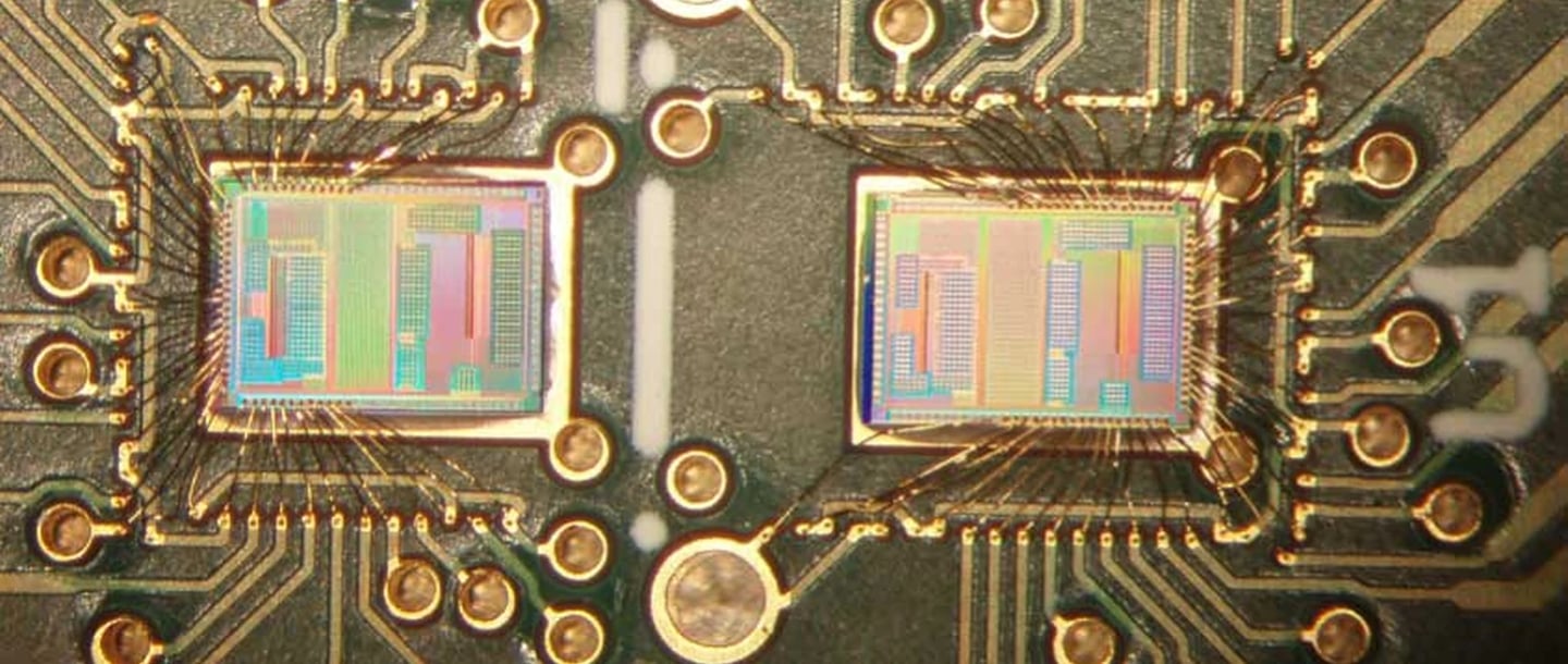
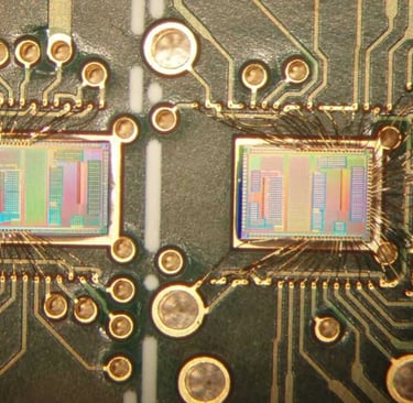
This image shows wire bonding on a dual-die MEMS semiconductor package, highlighting dense interconnect routing and the precision required to protect sensitive MEMS structures during assembly.
Wire Bonding for MEMS Devices: Packaging Challenges, Process Control, and Reliability Considerations
Microelectromechanical systems (MEMS) devices occupy a unique position in the semiconductor ecosystem. Unlike purely electronic integrated circuits, MEMS combine electrical functionality with mechanical structures such as beams, membranes, cavities, and moving masses. These hybrid characteristics introduce distinct challenges in backend assembly—particularly in wire bonding, which must provide reliable electrical interconnects without degrading sensitive mechanical elements.
Wire bonding remains the dominant interconnect technology for many MEMS devices due to its flexibility, cost effectiveness, and compatibility with a wide range of package types. However, standard wire bonding practices developed for logic or memory devices cannot be directly applied to MEMS without modification. MEMS devices require specialized consideration of die layout, pad location, mechanical isolation, stress management, and long-term reliability.
This article explores wire bonding for MEMS devices, focusing on the unique requirements of MEMS packaging, common wire bonding approaches, material choices, process risks, inspection strategies, and reliability considerations essential for successful MEMS assembly.
Why Wire Bonding Is Widely Used for MEMS
Despite the availability of alternative interconnect technologies such as flip-chip and wafer-level packaging, wire bonding remains widely used for MEMS devices for several key reasons.
First, wire bonding offers excellent design flexibility. MEMS dies often have irregular pad layouts dictated by sensor geometry, moving structures, or cavity placement. Wire bonding accommodates these non-uniform layouts more easily than area-array approaches.
Second, wire bonding supports low-to-medium volume production efficiently. Many MEMS applications—such as industrial sensors, medical devices, and automotive components—do not require the extremely high volumes that justify complex wafer-level interconnect schemes.
Third, wire bonding allows mechanical decoupling between the MEMS die and the package. By routing connections through compliant wire loops, mechanical stress transmitted from the package to the die can be reduced, which is particularly important for fragile MEMS structures.
Unique Packaging Requirements of MEMS Devices
MEMS devices differ from standard ICs in several fundamental ways that directly impact wire bonding.
Presence of Moving or Fragile Structures
Many MEMS devices include suspended beams, diaphragms, comb drives, or proof masses. These structures can be damaged by excessive vibration, mechanical shock, or localized stress during bonding.
Wire bonding processes must therefore be designed to:
Minimize die vibration during bonding
Avoid excessive ultrasonic energy coupling into the MEMS structure
Prevent tool contact near active mechanical areas
Cavities and Non-Planar Die Surfaces
MEMS dies often include etched cavities or non-planar topographies. These features can affect:
Bond pad accessibility
Tool clearance
Capillary or wedge stability during bonding
Special tooling and bond placement strategies are frequently required.
Sensitivity to Mechanical Stress
MEMS performance is often directly affected by mechanical stress. Packaging-induced stress can cause:
Sensor offset drift
Sensitivity changes
Long-term stability degradation
Wire bonding parameters must be carefully optimized to avoid introducing residual stress into the die.
Bond Pad Design and Location in MEMS Devices
Peripheral vs Central Pads
Many MEMS designs place bond pads at the periphery of the die to isolate wire bonding activity from sensitive structures. Peripheral pads simplify bonding and reduce risk but may increase die size.
In some compact designs, pads may be located closer to MEMS structures, increasing the need for:
Lower bonding force
Reduced ultrasonic energy
Careful loop routing
Pad Metallization Considerations
MEMS bond pads may use aluminum, gold, or copper metallization depending on process integration. Pad thickness and underlying layers must be sufficient to tolerate bonding forces without inducing cratering or delamination.
Thin pad stacks combined with fragile MEMS layers significantly narrow the bonding process window.
Wire Bonding Methods Used in MEMS Packaging
Ball Bonding
Ball bonding (thermosonic bonding) is commonly used for MEMS devices with compatible pad metallization. It offers:
High throughput
Consistent bond geometry
Good electrical performance
However, the combination of heat and ultrasonic energy must be carefully controlled to avoid MEMS damage.
Wedge Bonding
Wedge bonding is frequently preferred for MEMS devices due to:
Lower bonding temperatures
Directional control of wire placement
Reduced vertical force compared to ball bonding
Aluminum wedge bonding is particularly common in MEMS pressure sensors, accelerometers, and gyroscopes.
Wire Material Selection for MEMS Devices
Gold Wire
Gold wire is widely used in MEMS packaging due to its ductility and forgiving bonding behavior. It allows reliable bonds at relatively low ultrasonic energy and force, reducing mechanical stress on the die.
The primary disadvantages are cost and potential intermetallic growth at elevated temperatures.
Aluminum Wire
Aluminum wire is commonly used in MEMS wedge bonding, especially where aluminum pads are present. It offers good compatibility with MEMS metallization but requires higher ultrasonic energy to break surface oxides.
Copper Wire
Copper wire is less common in MEMS packaging due to its stiffness and higher bonding force requirements. While copper offers superior electrical performance, its mechanical characteristics increase the risk of MEMS damage unless processes are tightly controlled.
Ultrasonic Energy Management in MEMS Wire Bonding
Ultrasonic energy is one of the most critical parameters in MEMS wire bonding. Excessive ultrasonic energy can:
Excite MEMS structures
Induce microfractures
Alter mechanical calibration
To mitigate these risks, MEMS wire bonding processes often use:
Lower ultrasonic amplitudes
Shorter bond times
Optimized force-energy coupling
In some cases, bonding is performed with reduced or no ultrasonic energy, relying more heavily on force and temperature.
Loop Profile Design and Mechanical Isolation
Wire loop geometry plays a key role in protecting MEMS devices from package-induced stress.
Importance of Loop Compliance
Compliant loops help absorb:
Thermal expansion mismatch
Mechanical shock
Vibration transmitted through the package
Overly rigid or low-profile loops can transmit stress directly into the MEMS die, degrading performance over time.
Loop Height and Routing
MEMS packages often require customized loop profiles to:
Avoid cavities or moving structures
Prevent wire contact with caps or lids
Maintain consistent electrical characteristics
Advanced bonders enable programmable loop shaping to meet these requirements.
Encapsulation and Environmental Protection
MEMS devices may be packaged using:
Open cavities with lids
Gel encapsulants
Low-stress mold compounds
Wire bonding must be compatible with the chosen encapsulation method. For example, wire sweep during molding can be particularly damaging in MEMS packages where wires pass near sensitive structures.
Low-stress encapsulation materials and controlled mold flow are essential for maintaining wire integrity and MEMS performance.
Inspection and Testing of MEMS Wire Bonds
Inspection requirements for MEMS wire bonding extend beyond standard criteria.
Common inspection methods include:
High-magnification optical inspection
Wire pull and shear testing
Electrical continuity testing
Functional MEMS performance testing
Because MEMS devices are sensitive to mechanical stress, mechanical test results must be carefully interpreted to avoid test-induced damage.
Reliability Considerations for MEMS Wire Bonds
MEMS devices are often deployed in demanding environments, including automotive, industrial, and medical applications. Wire bonds must withstand:
Wide temperature cycling ranges
Mechanical vibration and shock
Long operational lifetimes
Reliability failures may manifest not only as electrical opens but also as gradual performance drift due to stress-induced changes in MEMS structures.
Long-term reliability testing is therefore essential to validate both wire bond integrity and MEMS functionality.
Common Failure Modes in MEMS Wire Bonding
Typical failure modes include:
Bond lifts due to insufficient energy
Heel cracks from excessive stress
Pad damage affecting MEMS layers
Wire fatigue under vibration
Many of these failures are latent and only appear after environmental stress testing.
Backend Manufacturing Support with Silicon Craft Technologies
Successfully wire bonding MEMS devices requires a deep understanding of both semiconductor backend assembly and MEMS-specific mechanical sensitivities. Silicon Craft Technologies provides engineering-driven backend manufacturing support tailored to these challenges.
With experience in MEMS device assembly, wire bonding process development, and reliability qualification, Silicon Craft Technologies works closely with customers to optimize bonding parameters, select appropriate materials, and mitigate mechanical risks. Their collaborative approach supports low-to-medium volume production, process troubleshooting, and transition from development to stable manufacturing.
By aligning wire bonding practices with MEMS device requirements, Silicon Craft Technologies helps ensure reliable electrical interconnects while preserving MEMS performance and long-term stability.
Conclusion
Wire bonding remains a vital interconnect technology for MEMS devices, offering flexibility, cost efficiency, and proven reliability. However, MEMS packaging introduces unique challenges that require careful control of bonding parameters, materials, and mechanical interactions.
Successful MEMS wire bonding depends on minimizing stress, managing ultrasonic energy, designing compliant loop profiles, and integrating bonding decisions with overall package architecture. With disciplined backend manufacturing practices and MEMS-aware process development, wire bonding can deliver reliable performance across a wide range of MEMS applications.
: