
WLP vs Traditional Packaging
A technical comparison of wafer-level packaging and traditional semiconductor packaging, examining process flows, electrical and thermal performance, reliability trade-offs, cost structures, and application-driven selection criteria for modern backend manufacturing.
Kiran
1/6/20265 min read
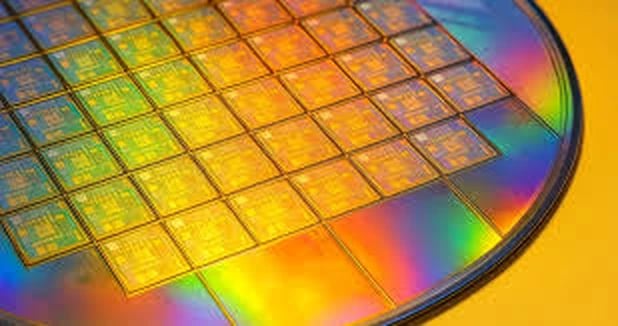
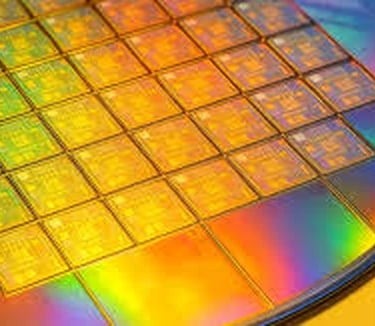
Close-up view of patterned semiconductor dies on a silicon wafer, illustrating wafer-level packaging and advanced microfabrication processes.
WLP vs Traditional Packaging: Process, Performance, and Manufacturing Trade-Offs
Introduction to Backend Packaging Evolution
Semiconductor packaging has transitioned from a purely protective function to a critical enabler of electrical performance, form factor reduction, and system-level integration. As device scaling at the transistor level encounters economic and physical limits, packaging architectures increasingly define achievable performance, cost, and reliability. Within this context, the comparison between wafer-level packaging (WLP) and traditional package-level approaches has become a central decision point for product designers, process engineers, and manufacturing strategists.
Both approaches are mature, widely deployed, and technically robust, yet they embody fundamentally different philosophies. Traditional packaging separates wafer fabrication and package assembly into discrete manufacturing stages, while WLP collapses much of the backend process directly onto the wafer before singulation. The implications of this difference extend across process flow, material selection, yield behavior, thermal performance, electrical parasitics, and long-term reliability.
Understanding the trade-offs between WLP and traditional packaging requires more than a surface-level comparison of size or cost. It demands an appreciation of backend process physics, equipment constraints, and the realities of high-volume manufacturing.
Defining Traditional Semiconductor Packaging
Traditional semiconductor packaging refers to package architectures in which the silicon die is first fabricated, then singulated, and finally assembled into a discrete package using leadframes, substrates, and mold compounds. This category encompasses wire-bonded packages, flip-chip packages, and substrate-based ball grid array (BGA) formats.
The conventional process flow begins with wafer fabrication and electrical wafer sort. After dicing, individual dies are attached to a package substrate or leadframe using die attach materials. Electrical interconnection is then achieved via wire bonding or flip-chip solder joints, followed by encapsulation, singulation (if panel-based), and final test.
This decoupled flow provides substantial flexibility. Die and package can be optimized independently, multiple die sizes can share a common package platform, and rework or binning strategies can be applied after dicing. These attributes have made traditional packaging the backbone of semiconductor manufacturing for decades.
Fundamentals of Wafer-Level Packaging
Wafer-level packaging shifts the center of gravity of backend processing upstream. In WLP, redistribution layers (RDL), passivation, under-bump metallization (UBM), and solder bump formation are completed while the die remains part of the intact wafer. Only after the package structure is fully formed does singulation occur.
This approach effectively eliminates the concept of a separate package body. The wafer itself becomes the package, with electrical interconnects routed to external solder balls through thin-film metallization stacks. Variants include fan-in WLP, where all interconnects remain within the die footprint, and fan-out WLP, where the package area is expanded using reconstituted wafers or panels.
By performing packaging at wafer scale, WLP leverages lithographic precision and parallel processing, but it also inherits the constraints and sensitivities of wafer-level manufacturing.
Process Flow Comparison: Wafer-Level vs Package-Level
The most fundamental distinction between WLP and traditional packaging lies in process sequencing and defect amplification behavior.
In traditional flows, backend yield losses occur after dicing, meaning that defects are localized to individual units. Scrap rates are therefore additive rather than multiplicative. In contrast, WLP processes are applied across the entire wafer. A systemic defect in RDL lithography, dielectric deposition, or bump formation can impact hundreds or thousands of dies simultaneously.
Wafer-level processing offers tighter dimensional control and alignment accuracy, but it demands extremely stable process windows. Any excursion in photoresist thickness, copper plating uniformity, or dielectric stress can propagate across the wafer, impacting final yield disproportionately.
From a manufacturing control perspective, WLP behaves more like front-end wafer fabrication, while traditional packaging retains the modularity of assembly-line manufacturing.
Electrical Performance and Signal Integrity
Electrical performance is often cited as a key advantage of WLP, particularly for high-frequency and low-power applications. The elimination of long wire bonds and thick organic substrates significantly reduces parasitic inductance and resistance. Shorter interconnect paths improve signal rise times, reduce noise coupling, and enhance power integrity.
Traditional wire-bonded packages, while highly reliable, introduce loop inductance that can degrade performance in RF, high-speed digital, and precision analog devices. Flip-chip packages mitigate many of these issues, but still rely on substrate routing that adds dielectric loss and impedance discontinuities.
WLP’s thin-film RDL structures enable controlled impedance routing and fine-pitch interconnects that are difficult to replicate in laminate substrates. However, this benefit is strongly application-dependent. For low-frequency or power-dominant devices, the electrical advantages of WLP may not translate into meaningful system-level gains.
Thermal Management Considerations
Thermal performance is a nuanced comparison between WLP and traditional packaging. WLP devices are thin, with minimal thermal mass, which can be advantageous for rapid heat dissipation into the PCB. However, the absence of a dedicated heat spreader or thick substrate can limit total heat flux capacity.
Traditional packages, particularly those using exposed pads, metal lids, or high-thermal-conductivity substrates, can manage higher power densities. The ability to integrate heat sinks or thermal vias at the package level provides additional design freedom.
In WLP, thermal paths are largely constrained by the silicon thickness, RDL stack, and solder joint interfaces. As power levels increase, these limitations can become critical, making traditional packaging more suitable for high-power or thermally aggressive applications.
Mechanical Reliability and Stress Management
Mechanical reliability behavior diverges significantly between the two approaches due to differences in material stacks and stress distribution.
WLP structures are thin and mechanically compliant, which can reduce certain stress concentrations. However, they are also more sensitive to board-level reliability issues such as solder joint fatigue, warpage, and coefficient of thermal expansion (CTE) mismatch between silicon and the PCB.
Traditional packages act as mechanical buffers. Mold compounds and substrates absorb stress, reducing strain transmitted to the die. This buffering effect improves robustness in harsh environments, including wide temperature cycling and mechanical shock.
From a reliability engineering standpoint, WLP often requires tighter control of board design, solder alloy selection, and assembly profiles to achieve equivalent field performance.
Yield Economics and Cost Structure
Cost comparisons between WLP and traditional packaging are rarely absolute. Instead, they are strongly influenced by volume, die size, yield maturity, and product mix.
WLP benefits from parallel wafer-scale processing, which can reduce per-unit cost at high volumes once processes are stabilized. The elimination of substrates, leadframes, and mold compounds also removes material costs associated with traditional packages.
However, initial yield learning curves for WLP can be steep. Because defects occur before singulation, early-stage yield losses are more expensive. Additionally, WLP is less tolerant of die size variation and process excursions.
Traditional packaging maintains cost efficiency across a wider range of volumes and product types. Its modular nature allows packaging houses to amortize equipment and tooling across many customers and devices, reducing financial risk.
Design Flexibility and Product Scalability
Traditional packaging offers superior design flexibility, particularly for multi-die integration, heterogeneous integration, and late-stage customization. Substrate routing enables complex interconnect topologies, multiple power domains, and integration of passive components.
WLP, especially fan-in variants, is inherently constrained by die footprint and routing density. While fan-out WLP addresses some of these limitations, it introduces additional process complexity and cost.
For products with long lifecycles, evolving requirements, or multiple derivative SKUs, traditional packaging often provides a more adaptable platform.
Application-Driven Selection Criteria
The choice between WLP and traditional packaging is rarely ideological. It is driven by application-specific requirements.
WLP is well-suited for mobile, wearable, and consumer electronics where form factor, low parasitics, and high volume dominate design priorities. Traditional packaging remains preferred for automotive, industrial, and high-power applications where reliability margins and thermal robustness outweigh size constraints.
In many portfolios, both approaches coexist, each optimized for different product segments.
Backend Manufacturing Support with Silicon Craft Technologies
Selecting an optimal packaging architecture is only one part of a successful product realization strategy. Execution at the backend manufacturing level ultimately determines whether theoretical advantages translate into production-worthy outcomes.
Silicon Craft Technologies operates at the intersection of wafer-level and package-level backend processes, supporting customers across a broad spectrum of packaging requirements. With experience spanning wafer-level processing, redistribution layer formation, bumping, and conventional assembly flows, Si-Craft brings an engineering-driven approach to backend manufacturing.
Rather than positioning packaging choices as one-size-fits-all solutions, Silicon Craft Technologies works collaboratively with customers to align process selection, reliability expectations, and manufacturability constraints. This includes process development, prototyping, and low-to-medium volume production environments where design decisions are still evolving.
By grounding packaging execution in process understanding and manufacturing discipline, Si-Craft Technologies supports backend semiconductor manufacturing strategies that balance performance, yield, and long-term reliability—regardless of whether wafer-level or traditional packaging architectures are ultimately selected.
If you want, I can next:
Add FAQ schema + HTML output
Generate a meta title, meta description, and internal linking plan
Rewrite this for pillar-cluster SEO alignment
Adapt tone for automotive, RF, or mobile-only audiences
Just tell me.